ZEISS Launches Crossbeam 550 Samplefab Scanning Electron Microscopes for Full Precision
ZEISS redefined the usability of focused ion beam (FIB) scanning electron microscopes (SEM) by launching ZEISS Crossbeam 550 Samplefab, a FIB-SEM system that could completely automate the TEM sample (lamella) preparation process. This solution provides recipe-driven automation for the day-to-day routine activities related to the preparation of samples for transmission electron microscopy (TEM) including bulk milling, lift-off-and-thinning processes performed on designated areas of the sample. The solution boasts of an automation yield that is more than 90% for the case of taking bulk lamellae and preparing them on the TEM grids – without any operator interruption. Automated checks allow operator involvement to prevent any lamellae loss from occurring during processing, thus ever-increasing lamella success rates to almost 100%.
TEM imaging allows the critical understanding of semiconductor device defect issues. However, the information contributed by the TEM analysis is reliant on the successful production within tolerances, of quality lamellae, within these lamellae, and at a swift pace. It is in response to this increasing demand within the industry that ZEISS created the ZEISS Crossbeam 550 Samplefab focused ion beam scanning electron microscope. Which employs the Gemini 2 electron column enabling the user to view the sample inside the SEM along with the FIB to tool to mill, thus obtaining optimal quality final lamina as well as end pointing where sample is thinner.
Latest Announcements by Industry Leaders
- Takashi Onodera, CEO of JEOL Ltd., a leader in electron microscopy systems, shared the company's ongoing commitment to pushing the boundaries of electron microscope technology. Onodera discussed their recent advancements in scanning electron microscopes (SEM) and transmission electron microscopes (TEM), which offer enhanced resolution and imaging speed.
- Dr. Michael Kaschke, former CEO of ZEISS, recently emphasized the role of electron microscopy in driving scientific progress. Kaschke announced that ZEISS would continue to develop high-performance electron microscopes that integrate advanced automation, AI, and machine learning to enhance imaging capabilities and data analysis.
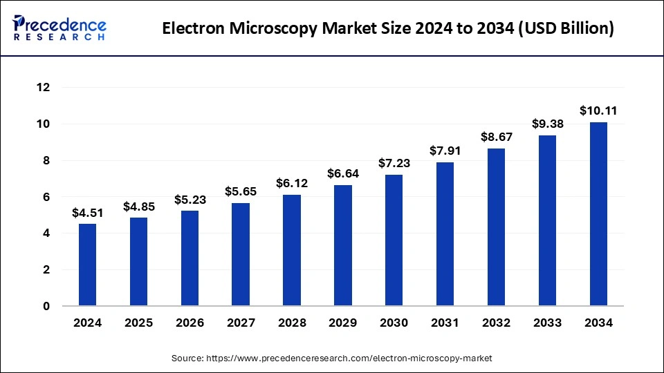
Electron Microscopy Market Size and Forecast 2024 to 2033
The global electron microscopy market size was valued at USD 4.51 billion in 2024 and is projected to surpass around USD 9.38 billion by 2033, expanding at a CAGR of 8% from 2024 to 2033.

Electron Microscopy Market Major Players
- Danish Micro Engineering (DME)
- Thermo Fisher Scientific
- Hitachi High Technologies Corp.
- JEOL Ltd.
- Leica Microsystems
- Nanoscience Instruments, Inc.
- Nikon Corp.
- Olympus Corp.
- Carl Zeiss
Recent Developments of Electron Microscopy Market
- In May 2024, Hitachi High-Tech announced the launch of the SU3900SE and SU3800SE High-Resolution Schottky Scanning Electron Microscopes that are designed for effortless observation of large and heavy weight specimens at the nanometric scales. The SU3900SE specimen stage extends the operating weights of specimens up to 5 kg thus enhancing the process efficiency. The a5-axis motorized stage is also included in the devices alongside camera navigation for easy usability.
- In February 2024, to explore the crystal structure with nanometric spatial resolution, the researchers employed unsupervised machine learning approaches, as well as scanning transmission electron microscopy (STEM). It leverages dimensionality reduction techniques such as non-negative matrix factorization and hierarchical agglomerative clustering. The research reveals an amorphous matrix and high-pressure annealed metallic glass crystalline precipitates, enabling unique bimodal investigations into material nanostructures.
- In February 2024, Scientists from the University of Illinois Urbana-Champaign have demonstrated that expensive aberration corrected optical systems are not necessary any more for obtaining resolution at the microscopic level. This achievement results from a newer technique called electron ptychography, which is an enhancement in the resolution of an electron microscope through computing and has dramatically grown the field of microscopy in the last 5-6 years.
We’ve prepared a service to support you. please feel free to contact us at sales@precedenceresearch.com | +1 804 441 9344