Electron Microscopy Market Size and Forecast 2026 to 2035
The global electron microscopy market size was calculated at USD 4.85 billion in 2025 and is predicted to increase from USD 5.23 billion in 2025 to approximately USD 10.83 billion by 2035, expanding at a CAGR of 8.36% from 2026 to 2035.
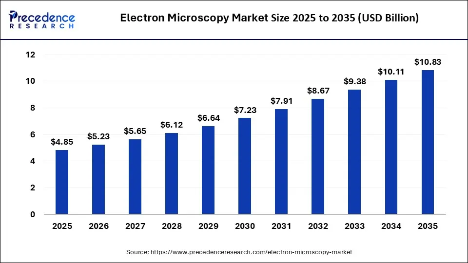
Electron Microscopy Market Key Takeaways
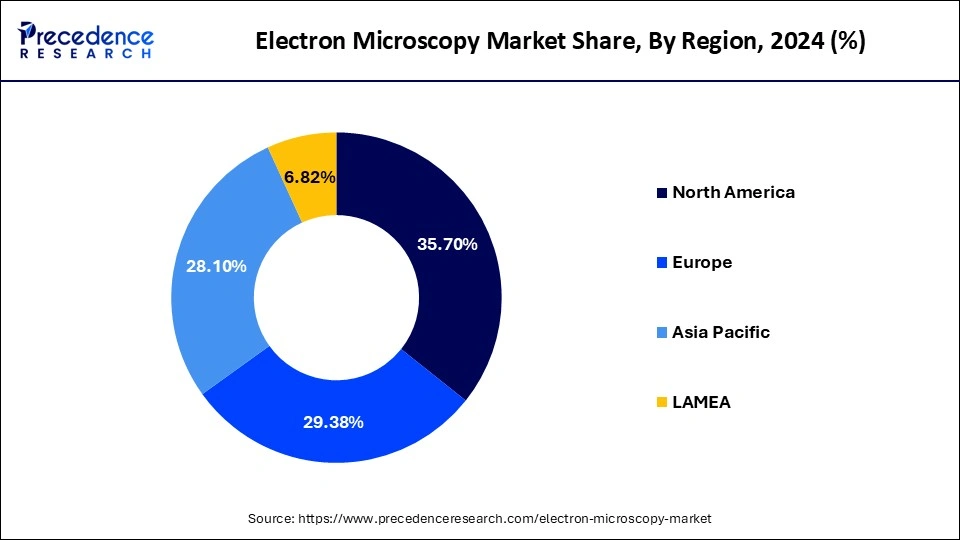
- North America generated more than 36% of revenue share in 2025.
- By Application, the lifesciences segment has accounted for a market share of 25% in 2025.
- By Type, scanning electron microscopes accounted market share of 79% in 2025.
Market Overview
Growing demand for nanotech research as well as an increase in funding are key market drivers for electron microscopy . Furthermore, expanding product applications in the electronics and pharmaceutical industries are expected to drive the market during the forecast period. Furthermore, advancements in resolution power and features such as the attachment of other devices, such as an energy x-ray dispersion spectroscope, are expected to drive market growth during the forecast period.
Scanning Electron Microscopes (SEMs) are popular due to their being widely used by small- to medium-sized R&D institutes and pharmaceutical companies. They offer data on surface topography and properties to researchers and quality control personnel, such as topography, chemical analysis, fractography, and so on.
Even though nanotechnology has applications in most areas of semiconductors, material sciences, and life sciences, which have a significant impact on any nation's economy, it encourages government organizations and other corporate enterprises to support R&D through public funding. The global market is expanding due to a variety of factors, including the fact that it is one of the most important devices for analyzing nanomaterials at the atomic scale in many pharmaceutical industries, medical devices , and multiple industrial verticals.
Microscopes are required for procedures such as lithography, coating, failure analysis, and detection in the manufacture of semiconductor devices . The rapid growth of the semiconductor industry in countries such as India and China because of outsourcing of electric manufacturing activities is a driving factor of the SEMs market.
Increased global attention on R&D for applications such as neurosciences, materials engineering, life sciences, nanotechnology, and the semiconductor industry would boost adoption of advanced and automated light microscopy such as scanning probe microscopes, analytical electron microscopes, and SEMs. These microscopes have imaging resolutions of up to 0.1 nm, which is essential for these precision manufacturing industries.
AI-Driven Electron Microscopy Reshapes Market Growth
Artificial Intelligence (AI) is revolutionizing the electron microscopy industry through its ability to automate image interpretation and speed up processes while providing immediate feedback on results that previously could only be achieved using manual methods. The efficiencies provided by AI-enhanced workflows allow for increased production in materials science, life sciences, and semiconductor applications by automating traditional tasks such as 3D reconstruction, noise reduction, and thus allowing for faster analysis times and decreased reliance on highly trained operators.
Recent advances in deep learning applied directly to SEM workflow enable researchers to use only 2D data to reconstruct 3D structures with very little manual input, vastly reducing analysis time and improving resolution accuracy. As AI continues to facilitate increased efficiency, unlock complex datasets, and further permeate the research and industrial sectors, their use will increase among both research institutions and high technology manufacturers, creating significant commercial growth opportunities and providing them with a competitive edge.
MarketScope
| Report Coverage | Details |
| Market Size in 2026 | USD 5.23 Billion |
| Market Size by 2035 | USD 10.83 Billion |
| Growth Rate from 2026 to 2035 | CAGR of 8.36% |
| Largest Market | North America |
| Base Year | 2025 |
| Forecast Period | 2026 to 2035 |
| Segments Covered | Type, End User, and Application |
| Regions Covered | North America, Europe, Asia-Pacific, Latin America, and Middle East & Africa |
Market Dynamics
Drivers
Rising scientific research
Electronic microscopes are frequently used in research labs, academic institutions, and nanotechnology centers. The structure of the sample can be examined in detail in these institutions to learn more about its function. Other bodies, such as industrial companies, can then build on and use the findings of scientific research centers. In a research laboratory, for example, an electron microscope may be used for particle analysis or material characterization. In biomedical research, electron microscopy can be used to investigate the molecular nature and mechanisms of disease, view the 3D structure of biological tissues or cells, determine protein structure, and observe viruses in a biological context. These findings can then be passed on to industry research centers, which will focus on utilizing the data to provide a solution. For instance, information about the nature of the disease could be used to develop medications to manipulate the results.
Higher refining and resolving power
The primary reason driving market expansion is electron microscopes' improved refining and resolving capacity, which provides enhanced output images extending up to several nanometers. Furthermore, the market is expanding because of increased demand for nanotechnology-based devices. Electron microscopes have a higher resolving power than light microscopes. They can see the structure of smaller devices. Electron microscopes are frequently used to investigate the ultrastructure of a variety of biological and inorganic specimens, including cells, microbes such as bacteria, biological macromolecules, biopsy samples, alloys, crystals, and metals. Quality control and analysis can also be performed using electron microscopes. Modern electron microscopes generate electron micrographs by capturing images with digital cameras and frame grabbers.
Restrains
High production cost
Electron microscopes high production and upkeep costs are the primary factors limiting their market expansion. Furthermore, the specialized conditions required for proper equipment operation are a major constraint in this industry. Because of technological advancements, people's attitudes towards microscopes have shifted. High-end microscopes, such as electron microscopes, scanning probe microscopes, and digital microscopes, are gradually losing favor with conventional microscopes due to their advanced features, higher resolution, and magnification power. However, the prices for these microscopes range from USD 25,000 to USD 2 million, making them prohibitively expensive for hospitals, pathologist laboratories, and small companies.
Opportunities
Rising technological advancement
The rapid advancement of nanotechnology is propelling the scanning electron microscope market forward. The growing consumer desire for smaller, more efficient devices at lower prices, combined with the growing demand for product miniaturization, has accelerated the development of nanotechnology in a variety of industries. Furthermore, the use of electron microscopes enables the creation of three-dimensional images in a variety of industries. Based on precise images, manufacturers can select optimal manufacturing materials, ensuring product stability and durability. These factors are anticipated to drive market growth during the forecast period.
The rising prevalence of various chronic diseases is expected to increase the demand for advanced R&D activities. As a result of the increased demand for R&D and funding, infrastructure in healthcare and other industries is improving. As a result, the growing number of laboratories in academic institutions and industries such as semiconductors and material sciences, among others, is expected to drive demand for scanning electron microscopes. The increasing use of scanning electron microscopes to review surface morphology and properties such as topography, fractography, and qualitative analysis, among other things, will support market growth.
Technology advancements in scanning electron microscopes enable the generation of data in digital form, which speeds up the instrument's operation. It also reduces the number of steps required for sample preparation. These factors are expected to contribute to the overall growth of the market during the forecast period.
Segments Insights
End User
In 2025, the industries segment is expected to dominate the electron microscopy market, driven by strong demand from sectors such as semiconductors, materials science, automotive, and advanced manufacturing. Industrial applications leverage electron microscopy for quality control, defect analysis, and nanostructure characterization, enabling manufacturers to maintain high-precision standards and accelerate innovation cycles. The increasing need for surface and material analysis in electronics and industrial research further reinforces this dominance. As global industries continue to adopt miniaturization and advanced materials, electron microscopy remains a cornerstone technology for ensuring product reliability and performance at scale.
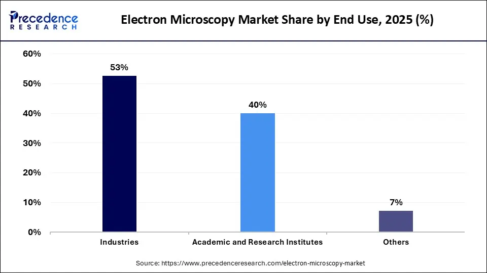
The academic and research institutes segment is anticipated to be the fastest growing end-user category in the electron microscopy market through 2025. Growth in this segment is propelled by expanding investments in life sciences, nanotechnology, and pharmaceutical research, where high-resolution imaging is critical for discovery and innovation. Universities, national laboratories, and research centers are increasingly acquiring advanced electron microscopes to support cutting-edge studies in biology, materials engineering, and environmental science.
Electron Microscopy Market Revenue, By End User, 2023-2025 (US$ Million)
| End User | 2023 | 2024 | 2025 |
| Industries | 2,204.9 | 2,370.4 | 2,555.3 |
| Academic and Research Institutes | 1,694.2 | 1,812.1 | 1,943.7 |
| Others | 311.6 | 331.4 | 353.4 |
Type Insights
The scanning electron microscopes dominate the electron microscopy market. The scanning electron microscope segment contributed the most revenue to the market and is expected to grow at a healthy CAGR due to an increase in demand for nanotechnology-based research. In medical science, SEMs are used to compare blood and tissue samples to determine the cause of illness and measure the effects of treatments on patients (while contributing to the design of new treatments). Typical applications include recognizing diseases and viruses, new vaccines and medicines being tested, and comparing tissue samples from patients in a control and test group testing samples over a patient's lifetime.
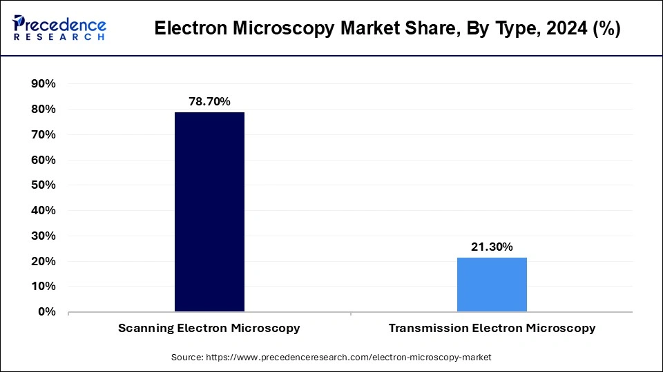
Electron Microscopy Market Revenue, By Type, 2023-2025 (US$ Million)
| Type | 2023 | 2024 | 2025 |
| Scanning Electron Microscopy | 3,308.8 | 3,552.4 | 3,824.5 |
| Transmission Electron Microscopy | 901.9 | 961.5 | 1,027.9 |
Application Insights
In 2025, the life science segment dominated the overall market, accounting for more than 25.0% of total revenue. Some of the factors contributing to the segment's large market share include the increasing prevalence of chronic diseases, which has led to increased R&D expenditure and demand for digital microscopes in the fields of life sciences and medicine. Life science, material science, nanotechnology, semiconductors, and other application segments are among those being studied in the industry.
Electron Microscopy Market Revenue, By Application, 2023-2025 (USD Million)
| Application | 2023 | 2024 | 2025 |
| Lifesciences | 1,053.5 | 1,123.6 | 1,201.6 |
| Material Sciences | 949.7 | 1,023.1 | 1,105.3 |
| Semiconductors | 1,543.6 | 1,653.0 | 1,775.1 |
| Nanotechnology | 423.8 | 460.0 | 500.7 |
| Others | 240.1 | 254.1 | 269.8 |
Material science was the second-largest end-use segment overall. SEM has become an established characterization tool in materials science. In materials science, SEMs are used for quality control, research, and failure analysis. Investigation and research on nanofibers and nanotubes, high mesoporous architecture, temperature superconductors, and alloy strength are all heavily reliant on nanofibers and nanomaterials.
U.S. Electron Microscopy Market Size and Growth 2026 to 2035
The U.S. electron microscopy market size was exhibited at USD 1.40 billion in 2025 and is projected to be worth around USD 2.99 billion by 2035, growing at a CAGR of 7.88% from 2026 to 2035.
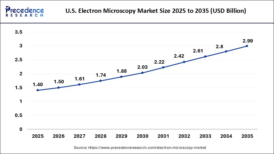
North America is a major regional market for scanning electron microscopes. The presence of major players specializing in product innovation, as well as rising expenditure on R&D activities, are driving regional market expansion. Furthermore, the presence of many educational institutions and scientific and technological facilities, particularly in the United States of America, creates a significant opportunity for a growing market.
U.S.
With a large number of prestigious universities, national laboratories, and technology driven industries, the United States leads the region. As electron microscopy is widely used in biomedical research, drug discovery, and advanced materials, there is a corresponding increase in demand for electron microscopy. In addition, the use of electron microscopes for semiconductor failure analysis and nanofabrication is becoming common, with government funded research projects and innovation through private companies encouraging frequent upgrades to technology. Furthermore, the availability of skilled researchers and technicians means that complex microscopy systems will be used efficiently, further establishing the United States' position as the leader in both academic and industrial applications of electron microscopy.
The expansion of research and development facilities in Europe has benefited this market in the region. The Asia Pacific region is also important in the market, with China, Japan, and India all contributing significantly to market growth. Increased government grants to develop the research and development sector, as well as rising demand for skinny wafers, particularly in the semiconductor industry, are some of the major factors driving market growth in the Asia Pacific region.
Why Asia Pacific Region is Fastest Growing in Electron Microscopy Market?
The Asia Pacific region is experiencing the most rapid growth in electron microscopy due to rapid industrialization, enhanced research capacity, and greater capacity for research and development. The demand for high-resolution imaging tools is expected to grow significantly due to the growth of the semiconductor manufacturing sector, increasing electronic manufacturing capacity, and the expansion of nanotechnology research capabilities. In addition, the expansion of the pharmaceutical and biotech sectors in APAC will continue to drive the use of electron microscopy as a tool for structural and cell analysis in this region. The growing awareness of the use of advanced analytical techniques and the increase in the amount of technical expertise will also contribute to the accelerated adoption of electron microscopy technology throughout developed and emerging economies within the Asia Pacific region.
China
China's aggressive investment in scientific infrastructure, advanced manufacturing capabilities, and the high demand for electron microscopes to support semiconductor development, material science engineering, and life science research make it the leading country driving growth in Asia Pacific's electron microscope market. The growing demand for nanotechnology and the growing demand for precision structural analysis in the manufacturing of electronics will also play a major role in the continuing growth of electron microscopy in Asia Pacific. Furthermore, as university-based research programs in China expand and the amount of technical expertise among Chinese researchers continues to grow, China will be a key driver of continued electron microscopy technological development in the Asia Pacific region.
Why is the Europe region experiencing the Notable growth?
The research community in Europe has a rich history of academic research, and the European Union supports IED to improve industrial operations. This includes research related to materials science, renewable energy research, and life sciences which all are reliant upon the use of electron microscopy as some of the major applications. As well there continues to also be encouragement of collaboration between countries through research programs allowing easy access to the use of advanced imaging facilities for all of the countries involved in each respective program. In addition, in both the manufacturing and pharmaceutical industries, there is stringent compliance with quality standards that requires the use of precise analytical tools. Therefore, the adoption of both transmission and scanning electron microscopes continues to grow at a steady pace.
Germany
While many European countries are experiencing continuous growth in their respective electron microscopy markets, Germany is by far the leader in all areas. The strong industrial research base and advanced engineering capabilities within Germany is one of the many reasons for the substantial growth experienced thus far by the electron microscopy industry in this country. The large research institute and university network within Germany fosters ongoing innovation for electron microscopy applications. The continued emphasis on precision manufacturing and optimizing the materials produced drives the demand for high-resolution imaging. Finally, the available skilled labor and commitment to applied research provides the ability for both industry and academic organizations in Germany to effectively utilize complex electron microscopy systems.
Why Latin America Is Emerging in Electron Microscopy Market?
Latin America's emerging electron microscopy market is driven by the region's steady growth in industrial and scientific research. Increasing demand for advanced imaging technologies is primarily due to many universities and public research institutions starting research programs. This region also shows increasing usage of advanced microscopy methods such as electron microscopy for materials sciences, mining, and life sciences. Although the electron microscope market in Latin America still lags behind the more developed regions, the region's growing research infrastructure, coupled with a growing number of people working in the electron microscope industry, are quickly building the region's electron microscopy technology base.
Brazil
Brazil has the most developed research infrastructure in Latin America and therefore has the largest academic base for conducting electron microscopy. Most research done with electron microscopy in Brazil is related to materials research, biotechnology, and agricultural research. In Brazil, government-sponsored research institutions and universities play a critical role in increasing the use of electron microscopy for research. The growing interest in and support of nanotechnology and biomedical research in Brazil is increasing the demand for high-resolution electron microscope imaging systems. In addition, Brazil is collaborating with international research networks and is continuously improving their laboratory facilities and equipment.
What's Causing the Growth of the Middle East Africa Region?
Middle East & Africa has been experiencing rapid growth in the electron microscopy sector due to large amounts of investment being put into developing the research infrastructure needed to diversify their economies. As more researchers focus on materials science, renewable energy and biomedicine, there is a greater demand for more sophisticated imaging technologies. Governments in the region are investing in higher education and research infrastructure, which is also encouraging scientists to use advanced analytical techniques. While there continues to be a limited amount of adoption of these types of instruments in the region, the growing number of people with the skills to operate these instruments and the increasing number of advanced laboratories will contribute to sustained growth in the region over time.
Saudi Arabia
Saudi Arabia has the highest level of investment in scientific R&D and higher education in the Middle East and Africa Region and therefore is the leader in the region's electron microscopy market. The use of electron microscopy is increasing rapidly in material engineering, renewable energy, and biomedicine, and many of the national research initiatives and funding that is available from universities to buy the necessary microscopy systems to complete these types of projects are financially supported. In addition, the government's emphasis on diversifying their economy through investment in technology therefore provides incentives for researchers to adopt high-end analytical techniques.
Recent Developments
- In July 2025, Thermo Fisher Scientific announced the launch of two new electron microscopes — the Scios 3 FIB-SEM for advanced site-specific analysis and the Talos 12 TEM to broaden research access at M&M 2025.
- In October 2025, Hitachi High-Tech introduced the SU9600 ultrahigh-resolution scanning electron microscope, offering sub-nano observation, automated workflows, and high throughput to support R&D in semiconductors and advanced materials.
- In March 2025, Shimadzu launched two models of the SUPERSCAN SS-4000 scanning electron microscope in Japan as the first products under the “Shimadzu by TESCAN” joint brand, optimizing low-acceleration and low-vacuum imaging.
Electron Microscopy MarketCompanies
- Danish Micro Engineering (DME)
- Thermo Fisher Scientific
- Hitachi High Technologies Corp.
- JEOL Ltd.
- Leica Microsystems
- Nanoscience Instruments, Inc.
- Nikon Corp.
- Olympus Corp.
- Carl Zeiss
Segments Covered in the Report
By Type
- Scanning Electron Microscopy (SEM)
- Transmission Electron Microscopy (TEM)
- Others
By End User
- Industries
- Academic and Research Institutes
- Others
By Application
- Lifesciences
- Material Sciences
- Semiconductors
- Nanotechnology
- Others
By Geography
- North America
- Europe
- Asia-Pacific
- Latin America
- Middle East and Africa
For inquiries regarding discounts, bulk purchases, or customization requests, please contact us at sales@precedenceresearch.com
Frequently Asked Questions
Ask For Sample
No cookie-cutter, only authentic analysis – take the 1st step to become a Precedence Research client
 Get a Sample
 Table Of Content


 sales@precedenceresearch.com
 +1 804-441-9344
 Schedule a Meeting