


Semiconductor Manufacturing Equipment Trends, Leading Companies, Company Revenue / Sales Performance, Manufacturing Yield, Fab Capacity, Export & Import Dynamics, Supply Chain Analysis, Competitive Landscape, and Growth Forecast
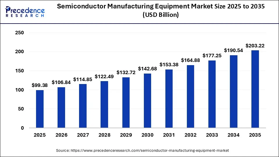
According to semiconductor and electronics specialist Laxmi Narayan, the semiconductor manufacturing equipment market is valued at USD 106.84 billion in 2026 and is forecast to reach USD 203.22 billion by 2035, reflecting a CAGR of 7.42%. Leading semiconductor manufacturing equipment market companies, including asml, applied materials, tokyo electron limited, lam research, kia corporation, are strengthening their presence across key segments such as equipment type, dimension, application, product type, supply chain participant.
Source: https://www.precedenceresearch.com/semiconductor-manufacturing-equipment-market
 Get a Sample
 Table Of Content


What is Semiconductor Manufacturing Equipment Market Size?
The global semiconductor manufacturing equipment market size accounted for USD 99.38 billion in 2025, and is projected to hit USD 106.84 billion by 2026, and is expected to reach around USD 203.22 billion by 2035, expanding at a CAGR of 7.42% from 2026 to 2035.
Market Highlights
- Asia Pacific led the global market with the highest market share of 68% in 2025.
- By equipment type, the front end equipment segment has held the largest market share in 2025.
- By dimension, the 3D segment captured the biggest revenue share in 2025.
- By application, the semiconductor fabrication plant/foundry segment registered the maximum market share in 2025.
How is AI Contributing to the Semiconductor Manufacturing Equipment Market?
AI is transforming the semiconductor sector by automating process control, accurately measuring wafer inspection, and improving defect classification. Predictive models that are built on machine learning help in reducing the maintenance time by notifying the personnel beforehand. Moreover, AI-powered analytics will yield and process parameters related to production to the maximum. It also does a good job in accelerating material discovery, chip design, and management of supply chains. Thus, AI, by combining deep learning and BD (data-driven) optimization, results in the semiconductor fabrication process with higher precision, less waste, and therefore, continuous innovation.
Semiconductor Manufacturing Equipment Market Growth Factors
One of the key factors driving the growth of global semiconductor manufacturing equipment market is the surge in demand for consumer electronics. In the consumer electronics industry, there is a growing demand for sophisticated and miniaturized semiconductor components and parts. In addition, the technological advancements and adoption of innovative technologies such as artificial intelligence and blockchain are supporting the growth and development of global semiconductor manufacturing equipment market. Furthermore, the semiconductor manufacturing equipment market will develop as a result of technological advancements in extreme ultraviolet lithography equipment. For example, ASML reported in February 2019 that it had delivered 18 high end lithography machines to Taiwan Semiconductor Manufacturing Company for $2.16 billion.
The COVID-19 pandemic had negative impact on the growth of global semiconductor manufacturing equipment market. This is due to the supply chain disruption and halt of manufacturing units globally. According to research released in February by the Semiconductor Industry Association, the COVID-19 pandemic could have long term commercial implications outside the China. Companies' 2020 revenues may show the impact of lower demand.
One of the major applications of the semiconductor equipment and devices are the manufacturing of consumer electronics. In addition, the growing penetration of smartphones and wearable devices are also boosting the semiconductor manufacturing equipment market growth. Smartwatch unit sales increased to 141 million in 2018, up from 75 million in 2017, as per the Consumer Technology Association, which is projected to benefit the semiconductor manufacturing equipment market. According to the GSM 2019 Report, mobile subscribers are predicted to increase from 5.1 billion in 2018 to 5.8 billion in 2025. As a result, the global semiconductor manufacturing equipment market is expected to expand in upcoming years.
Another trend that is shaping the global semiconductor manufacturing equipment market is the rising usage of hybrid and electric vehicles. Electric cars represented for 2.6% of the worldwide auto sales and around 1% of global automobile stock in 2019, according to the International Energy Agency and this trend will continue at a 40% annual growth rate. The large number of semiconductors are used as parts and components in electric cars. Thus, this factor is contributing towards the expansion of global semiconductor manufacturing equipment market.
Market Outlook
- Industry Growth Overview: The rapid advancement in digital transformation, along with the innovations in AI-driven chip manufacturing, is creating new designs for semiconductor equipment that are highly efficient, scalable, and competitive in the global market.
- Sustainability Trends: The semiconductor industry integrates environmental sustainability with operational performance by focusing on green fabs, energy-efficient plasma tools, and water recycling systems to comply with global sustainability standards in production.
- Global Expansion: The global collaboration and local production strategies are transforming the supply chains worldwide, giving the regional ecosystems the power to be resilient, technologically self-sufficient, and to have the advanced fabrication capabilities of other regions.
- Major Investors: The global players are investing heavily in companies that are leading the way in next-gen lithography, AI inspection systems, and quantum-ready equipment, thus advancing the development of scalable, future-proof semiconductor manufacturing.
- Startup Ecosystem: Startups that are coming up are working with the use of deep learning, robotics, and nanoscale precision tools, thus changing the landscape of traditional manufacturing and speeding up the process of chip fabrication automation and defect detection.
Market Scope
| Report Coverage | Details |
| Market Size in 2025 | USD 99.38 Billion |
| Market Size in 2026 | USD 106.84 Billion |
| Market Size by 2035 | USD 203.22 Billion |
| Growth Rate from 2026 to 2035 | CAGR of 7.42% |
| Largest Market | Asia Pacific |
| Fastest Growing Market | Europe |
| Base Year | 2025 |
| Forecast Period | 2026 to 2035 |
| Segments Covered | Equipment Type, Dimension, Application, Product Type, Supply Chain Participant, and Region |
| Regions Covered | North America ,Asia Pacific,Europe, Latin America, Middle East and Africa |
Segments Insights
Equipment Type Insights
The front end equipment segment dominated the semiconductor manufacturing equipment market in 2025. There are several market players who are selling front end equipment in the global semiconductor manufacturing equipment market. As per the Semiconductor Industry Association, developing and producing semiconductors account for the majority of chip's value. Thus, this factor is driving the segment growth.
The back end equipment segment is fastest growing segment of the semiconductor manufacturing equipment market in 2024. The back end equipment segment growth is being driven by the stringent government regulations. In addition, the launch of new and innovative products is boosting the growth of the segment.
Dimension Insights
The 3D semiconductor manufacturing equipment segment dominated the semiconductor manufacturing equipment market in 2025. One of the major factors boosting the growth of the segment is technological developments in manufacturing semiconductor devices and equipment. The 3D integrated circuits are highly used in the semiconductor manufacturing equipment market. Thus, this factor is expected to boost the growth of semiconductor manufacturing equipment market, as design and development of 3D integrated circuits will shape the market in a new way.
The 2D and 2.5D segment is fastest growing segment in 2024. The reduced length and reusability are enabled by the 2D and 2.5D dimensions, leading to decreased time and system cost. This factor is accelerating the expansion of the global semiconductor manufacturing equipment market.
Application Insights
The semiconductor fabrication plant/foundry segment dominated the semiconductor manufacturing equipment market in 2025. The demand for semiconductor is growing rapidly in various industries such as medical devices, consumer electronics, and automotive. This factor is driving the usage of semiconductor manufacturing equipment for semiconductor fabrication plant or foundry.
The semiconductor electronics manufacturing and test home segments is fastest growing segment of the semiconductor manufacturing equipment market in 2024. One of the significant factors driving the growth of the segment is growing awareness regarding the testing of semiconductor and its parts. In addition, the growing awareness about the strict government regulations regarding testing of semiconductor manufacturing equipment is supporting the growth of global semiconductor manufacturing equipment market.
Regional Insights
Asia Pacific Semiconductor Manufacturing Equipment Market Size and Growth 2026 to 2035
The Asia Pacific semiconductor manufacturing equipment market size is estimated at USD 67.58 billion in 2025 and is predicted to be worth around USD 138.19 billion by 2035, at a CAGR of 6.72% from 2026 to 2035.
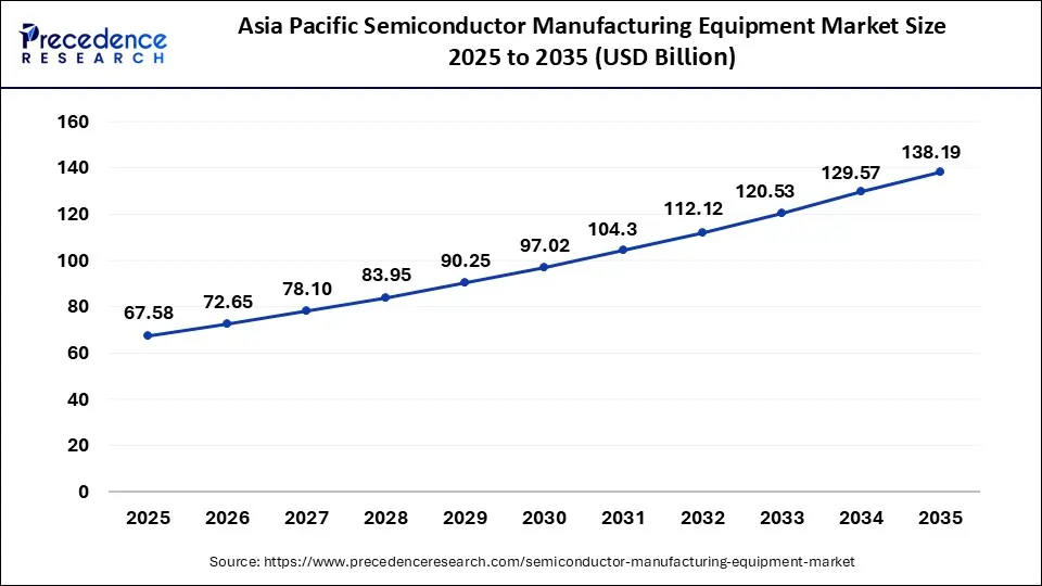
Asia-Pacific dominated the semiconductor manufacturing equipment market in 2025. China dominated the semiconductor manufacturing equipment market in Asia-Pacific region. The presence of key market players especially in emerging nations such as China and Japan are driving the growth of semiconductor manufacturing equipment market in the region. As per the International Trade Administration, Korea and Japan were the biggest exporters of semiconductor manufacturing equipment in 2016. Thus, the Asia-Pacific semiconductor manufacturing equipment market is expected to expand in near future.
China Semiconductor Manufacturing Equipment Market Trends
China is a semiconductor equipment market that goes through a big change driven by a series of innovations, fusing mostly automation, AI-based process optimization, and high-quality fabrication methods. The main goal of these innovations is to build up the domestic infrastructure as well as to make the country less dependent on imports. The country also aims at eco-friendly production practices, upskilling of the staff, and working on next-gen chipmaking technology to strengthen its role as a major player in the global semiconductor value chain.
What Explains North America's Rise as the Fastest-Growing Semiconductor Equipment Market?
North America is swiftly emerging as a growth hub for the semiconductor production equipment market because of huge investments and state-sponsored programs to support domestic chip manufacturing. The U.S. especially stands out as the leader in this burgeoning era for North America spurred by the CHIPS and Science Act, which has provided over $50 billion to stimulate chip production and innovation.
Major players in the industry such as Intel, TSMC, and Samsung have announced or begun construction of advanced fabs in states like Arizona, Ohio, and Texas. The increase in local fabrication projects is triggering demand for advanced production equipment, leading North America to emerge as an important growth area for semiconductor equipment suppliers.
United States Semiconductor Manufacturing Equipment Market Trends
The United States is the leader in the semiconductor manufacturing innovation sector, where it has utilized a combination of automation, artificial intelligence, and precision engineering. The continuous investments in chip design and fabrication have built up the capabilities of the domestic market. The ecosystem is giving support to the innovations in lithography and metrology tools with a strong emphasis on risk reduction in the supply chain and the establishment of environmental sustainability through digital monitoring and resource-efficient manufacturing techniques.
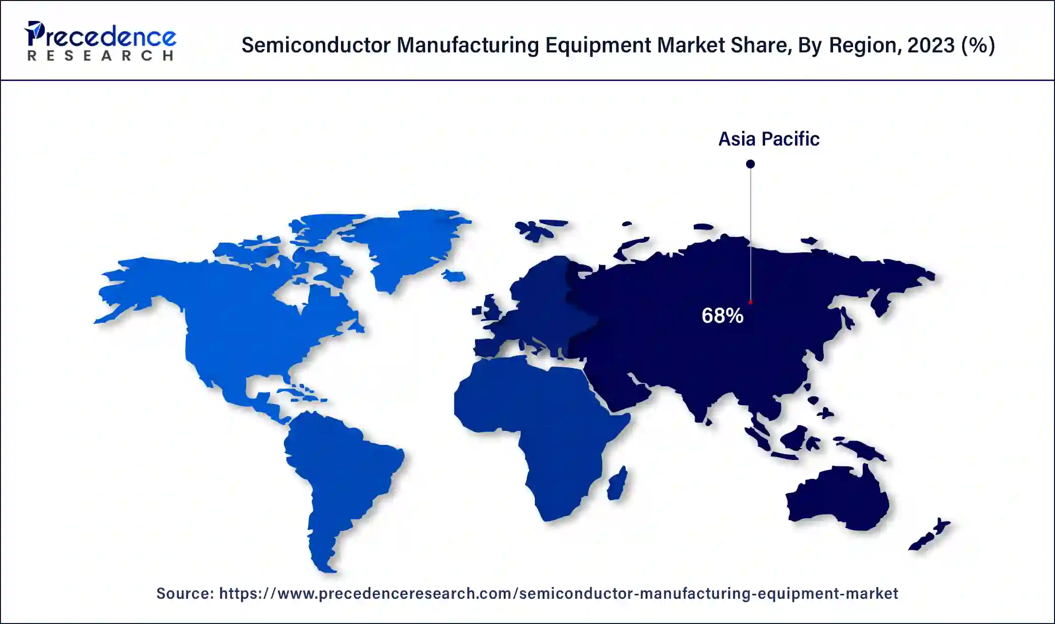
Europe, on the other hand, is expected to develop at the fastest rate during the forecast period. The UK dominates the semiconductor manufacturing equipment market in Europe region. The growing investments for manufacturing semiconductor equipment are driving the growth of semiconductor manufacturing equipment market in Europe region. In addition, good trade relations with other nations are paving way for expansion of Europe semiconductor manufacturing equipment market.
Germany Semiconductor Manufacturing Equipment Market Trends
Germany is on top of the European semiconductor equipment technology with its solid industrial base and engineering know-how. Smart automation, robot integration, and advanced materials research are the focus of its activities. The automotive industry's going electric increases the need for fast and efficient chip manufacturing. The up-to-date and optimized production processes ensure that the whole manufacturing area has both a competitive edge and low energy consumption.
Value Chain Analysis
- Raw Material Procurement: Obtaining ultra-pure silicon, metals, and specialty gases necessary for the production of wafers.
Key Players: Shin-Etsu Chemicals, Sumitomo Chemicals, and Merck Group - Wafer Fabrication (Front-end): The production of silicon wafers integrated with circuits using very clean and controlled conditions.
Key Players: Applied Materials, Tokyo Electron (TEL), and Lam Research - Photolithography and Etching: The application of light to mold the patterns of the circuit onto the silicon wafer, and subsequently carrying out the removal of unnecessary materials either by plasma or chemicals.
Key Players: ASML, Applied Materials, and Lam Research - Doping and Layering Processes: Making the circuit layers conductive and insulating them by introducing dopants and deposition of the thin films, respectively. Key players: Applied Materials and Lam Research
- Testing and Quality Control: Chips and wafers are checked for defects, and their performance is verified; only then can the goods be shipped.
Key Players: Amkor Technology, JCET, Teradyne, and Advantest
Competitive Landscape
The semiconductor manufacturing equipment market is emerging with the modern requirements in the semiconductor industry, as developments across the electrifying sector are acknowledging smart innovations in their products. Advanced packaging and AI chips are the blockbusters of the market that lead to growth, expansion and development. These three pillars are promoting the market with fundamental trends followed by smart deployments in the sectors. The market leaders such as ASML, Applied Materials, Tokyo Electron Limited (TEL), Lam Research, and KLA Corporation are unlocking new potential of the market.
Company Profiles
ASML
- HQ: Veldhoven, Netherlands.
- Founded: 1984
- Ownership: Supplier of EUV lithography systems and multinational corporation.
- Business Overview: The company is popular for its EUV lithography systems that have gained massive client engagement and profit. Its best-in-class engineering and build-up of critical machines indicate the dedication of the company to this market.
- Products: TWINSCAN NXE, TWINSCAN NXT, inspection systems, etc.
- Geographic Presence: ASML's footprint covers 60 locations with 44,000 dedicated employees.
- Revenue: The company's 2026 Q2 net sales are reaching €9.326 billion following the 2026 Q1 profit of €8.767 billion.
- Recent Development: In May 2026, ASML and Tata Electronics announced their partnership to welcome chip manufacturing in India. This agreement is noted to be profitable for the Indian semiconductor business.
- Key Strategies: Company's enthusiast for discovering the needs in the semiconductor industry frames the best business profit for the company and the semiconductor industry as well.
Applied Materials
- HQ: Santa Clara, California.
- Founded: 1967
- Ownership: Supplier of semiconductor-based services, software and equipment.
- Business Overview: Applied's business is to deliver the essential software, services and equipment to the semiconductor giants seeking seamless manufacturing operations to meet advanced unified circuits and displays. The precision and quality in its products and services attract giants that propel the company's business.
- Products: Automation software, modern chipmaking tools, etc.
- Geographic Presence: The company's offices, business footprint and manufacturing contribution cover Malaysia, Philippines, Taiwan, South Korea, Japan and China.
- Revenue: The company's 2026 Q1 revenue is $7.01 billion, and by Q3 it reached $9.12 billion by July 2026.
- Key Strategies: Applied strategize to announce its enhanced skills to maintain its client business and position in the market.
Tokyo Electron Limited (TEL)
- HQ: Minato City, Tokyo, Japan.
- Founded: 1963
- Ownership: Electronics company (previously a trading company).
- Business Overview: TEL's production of robust equipment for wafer fabrication contributes to semiconductor leaders, whereas its supply strength and own electronic business are strong backing for the company's financial status.
- Products: Decomposition systems, cleaning systems, and other equipment.
- Geographic Presence: The company's reach is across Europe, Asia and North America.
- Revenue: TEL's 2025 revenue was $16.048 billion, and its sales revenue in 2026 reached ¥2,443.5 billion.
- Recent Development: In April 2025, IBM and TEL extended their contract for modernizing semiconductor technology. This will double the power of research and development since the tuning of both companies is an advantage to the tech mission, which is eventually a profit to the market as well.
- Key Strategies: TEL's maturity in transitioning its production and supply value highlights the upgrading strategy that will benefit the company's expansion business.
Lam Research
- HQ: Fremont, California, United States.
- Founded: 1980
- Ownership: Supplier to semiconductor industries.
- Business Overview: Lam's famous services and robust wafer-fabrication equipment highlight the quality and potential of tech-influenced tools visible in the semiconductor innovation portfolio. The company acts as a responsible associate to semiconductor giants' innovation.
- Products: Plasma etch, thin film deposition, wafer cleaning tool and other systems.
- Geographic Presence: The company's operations are across Europe, Asia and the United States.
- Revenue: Lam's 2025 revenue was $18.44 billion, and in 2026 it reached $23.23 billion.
- Recent Development: In September 2026, Lam announced its profitable offering of 240-hour training for individuals to graduate in mechanical assembly and electronics jobs that will stimulate employment and market position with a massive number of employees for the semiconductor business.
- Key Strategies: The company's strategy is to shape research and development space for thin film deposition and plasma etch. The billions in funding position the company at the top of the market.
KLA Corporation
- HQ: Milpitas, California, USA.
- Founded: 1975
- Ownership: Technology company.
- Business Overview: The company's robust tools, software, and hardware precision unlock the portfolio position. KLA is a supplier of wafer fabrication equipment that indicates fine engagement with the semiconductor leaders.
- Products: Metrology systems, wafer inspection, KLA instruments, etc.
- Geographic Presence: The company's business is across Europe, Asia, North America and the Middle East.
- Revenue: KLA's current annual revenue is $13.58 billion.
- Key Strategies: The company's core strategy is to promote AI infrastructure and attract modern packaging as its profitable business.
Recent Developments
- In March 2025, S-based Yield Engineering Systems (YES), a leading manufacturer of process equipment for artificial intelligence (AI) and high-performance computing (HPC) semiconductor solutions, has announced the shipment of the first commercial VeroTherm Formic Acid Reflow tool to a leading global semiconductor manufacturer from its manufacturing facility. (Source: https://www.business-standard.com)
- In November 2024, ULVAC, Inc., the world's leading comprehensive vacuum manufacturer, launches technology center PYEONGTAEK for next-gen semiconductor manufacturing equipment in South Korea. Technology Center PYEONGTAEK will leverage the ULVAC Group's extensive human resources and expertise to promptly deliver high-quality manufacturing equipment that meets customer needs while also enhancing technical support.
(Source: https://en.antaranews.com) - Lam Research Corporation developed VantexTM, the most sophisticated dielectric etch process built specifically for Sense.i, the most intelligent etch platform, in January 2021. The ground-breaking architecture which is founded on etch leadership, gives current and next generation NAND and DRAM memory devices better performance and expandability.
- R&D Altanova Inc. a prominent provider of consumable test interface boards and interconnects for high end usage, was bought by Advantest Corporation in November 2021. Advantest's test and measurement solutions were to be expanded across the ever-changing semiconductor value chain as a result of the acquisition.
- KLA Corporation declared the Surfscan SP7XP water and the PWG5TM wafer geometry system, a flaw inspection system in December 2020. These innovative technologies are designed to solve some of the most difficult challenges in the manufacturing of advanced memory and logic integrated circuits.
- The Electron Beam Area Inspection System GS1000 will be available in December 2021, according to Hitachi High Tech Corporation. Through the use of a common platform based on established high speed inspection SEMs and knowledge of industry leading CD-SEM technology and high speed and huge measurements, the newly built instrument delivers precise and speedy e-beam inspection.
Segments Covered in the Report
By Equipment Type
- Front end Equipment
- DUV Lithography
- EUV Lithography
- Etching
- Chemical Mechanical Planarization
- Single-Wafer Spray System
- Single-Wafer Cryogenic System
- Batch Immersion Cleaning System
- Batch Spray Cleaning System
- Scrubber
- PVD
- CVD
- Lithography Equipment
- Water Surface Conditioning Equipment
- Wafer Cleaning Equipment
- Deposition Equipment
- Other
- Back end Equipment
- Assembly and Packaging
- Dicing
- Metrology
- Bonding
- Water Testing
By Dimension
- 2D
- 2.5 D
- 3 D
By Application
- Semiconductor Fabrication Plant/Foundry
- Semiconductor Electronics Manufacturing
- Testing Home
By Product Type
- Memory
- Foundry
- Logic
- MPU
- Discrete
- Analog, MEMS and Others
By Supply Chain Participant
- Introduction
- IDM Firms
- OSAT Companies
- Foundries
By Region
- North America
- Latin America
- Europe
- Asia-pacific
- Middle and East Africa
For inquiries regarding discounts, bulk purchases, or customization requests, please contact us at sales@precedenceresearch.com
Frequently Asked Questions





Ask For Sample
No cookie-cutter, only authentic analysis – take the 1st step to become a Precedence Research client
 Get a Sample




 sales@precedenceresearch.com
 Schedule a Meeting