What is the Flip Chip Market Size?
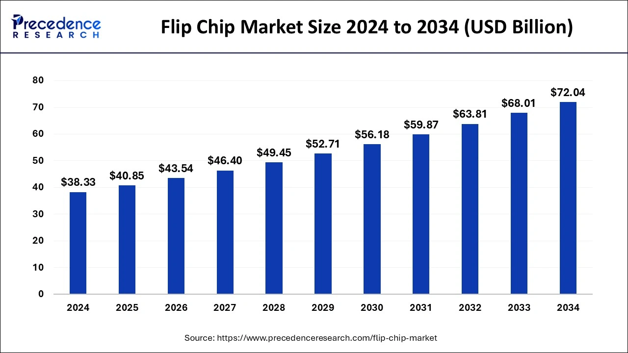
The global flip chip market size is calculated at USD 40.85 billion in 2025 and is predicted to increase from USD 43.54 billion in 2026 to approximately USD 76.18 billion by 2035, expanding at a CAGR of 6.43% from 2026 to 2035.

Flip Chip MarketKey Takeaways
- In terms of revenue, the global flip chip market was valued at USD 40.85billion in 2025.
- It is projected to reach USD 76.18 billion by 2035.
- The market is expected to grow at a CAGR of 6.43% from 2026 to 2035.
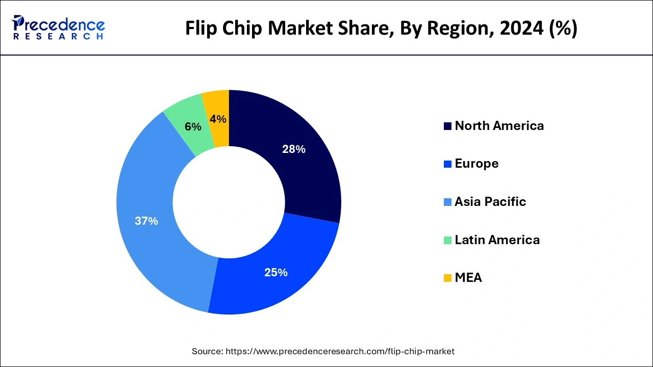
- Asia Pacific dominated the market with the largest market share of 37% in 2025.
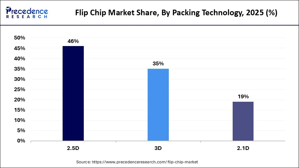
- By packaging technology, the 2.5D segment held the largest market share of 46% in 2025.
- By bumping, the gold stud bumping segment captured the biggest market share in 2025.
- By end use, the automotive segment holds the largest market share in 2025.
Flip Chip MarketGrowth Factors
- The flip chip market is experiencing growth driven by various factors. Despite requiring additional processing steps, traditional capillary-flow underfills are being enhanced to reduce cure time, contributing to market expansion.
- Advanced flip-chip interconnect technology offers improved performance for high-speed systems, productivity gains over manual wire bonding, and benefits such as self-alignment during die joining and reduced lead inductance, fostering market growth.
- Flip-chip configuration advantages, particularly for LEDs on dielectric substrates and microcavity LEDs, are propelling the growth of the flip chip market due to better thermal dissipation and simplified current conduction paths.
- In microelectronics packaging, flip chips are widely adopted due to integration demands. Efforts to detect solder bump defects, such as revising flip chip analytical models, are driving market growth.
- Packaging technologies like wire bonds and flip chips are versatile and ubiquitous, meeting diverse application needs and stimulating market growth.
- Flip chip technology is crucial for new complex system architectures and high-density packaging, particularly in sensor and pixel devices. Ensuring the availability of bumped wafers/dice at low cost, high yield, and quality levels is vital for market expansion.
Market Scope
| Report Coverage | Details |
| Growth Rate from 2026 to 2035 | CAGR of 6.43% |
| Market Size in 2025 | USD 40.85 Billion |
| Market Size in 2026 | USD 43.54 Billion |
| Market Size by 2035 | USD 76.18Billion |
| Largest Market | Asia Pacific |
| Base Year | 2025 |
| Forecast Period | 2026 to 2035 |
| Segments Covered | By Packaging Technology, By Bumping Technology, and By End-use |
| Regions Covered | North America, Europe, Asia-Pacific, Latin America, and Middle East & Africa |
Market Dynamics
Drivers
Engineering validation and performance enhancement
The advantages of flip chip packaging over wire bonding have been demonstrated through engineering analysis and experimental validation. Electrical modeling predicts a significant performance increase of 5-9% for microprocessors when transitioning from wire bond to flip chip packaging. Actual speed testing and statistical analysis on matched chips confirm a median speed gain of 8.1%.
Furthermore, the development of high-performance flip-chip light-emitting diodes (FCLEDs) with a Ni/Ag metallic film as a high reflectivity mirror has shown promising results. Investigating geometric electrode patterns and analyzing their impact on current spreading in the active region has led to improvements in current-voltage characteristics and light emission patterns. These advancements contribute to the growth of the flip chip market by enhancing performance and expanding application possibilities.
Miniaturization and increased power drive
As the electronics packaging industry trends towards miniaturization, there's a growing demand for higher I/O within smaller printed circuit board areas. Simultaneously, the power output of chips has been steadily increasing, leading to higher watt densities. These dynamics have propelled the adoption of area array packages like ball grid array (BGA), chip scale packages (CSP), and flip chips. Flip chip designs offer advantages such as higher I/O density, improved electrical performance, cost reduction, and enhanced thermal management. Particularly, the need for better thermal performance due to increasing chip power densities has drawn significant interest from board designers and thermal engineers.
Innovations enhancing the thermal performance of FC-PBGA packages, including underfill thermal conductivity and controlled collapse chip connection (C4) pitch, alongside improvements in package to printed wiring board (PWB) interconnection through thermal balls, have fueled market growth. Additionally, ceramic substrate FC-CBGA packages are gaining traction for their ability to deliver improved electrical performance, thanks to the design flexibility enabled by a large number of layers and small vias, facilitating effective power and ground planes. These advancements are key drivers propelling the growth of the flip chip market.
Restraints
Manufacturing constraints
The advancement of bump technology has been crucial in meeting the escalating demands for power and signal connection density in memory, high-performance computing, and mobile computing devices. However, as the industry pushes towards smaller bump pitches to accommodate these requirements, challenges in manufacturing arise. The transition from lead-free bumps to copper pillars and subsequently to copper microbumps marks a significant progression in flip-chip interconnect technology. Nevertheless, the ongoing reduction in pitch sizes poses hurdles in bumping and bonding processes, thereby restraining the growth potential of the flip chip market.
Cost challenges
Flip chip packages, while offering advantages for area-constrained applications, face several limitations that impede their widespread adoption. The additional cost of wafer bumping and high substrate costs make them less cost-effective for broader applications. Their lack of a carrier renders them unsuitable for easy replacement or unaided manual installation, further limiting their versatility. Moreover, the requirement for very flat mounting surfaces presents challenges in arrangement and maintenance, particularly as boards undergo heating and cooling cycles, restricting the maximum device size.
Additionally, the stiffness of short connections poses concerns regarding thermal expansion matching between the chip and supporting board, risking connection cracks. Although underfilled materials mitigate differences in the coefficient of thermal expansion (CTE) between the chip and board, these constraints collectively hinder the growth potential of the flip-chip market. Addressing these challenges will be crucial to expanding the market reach of flip chip technology.
Opportunities
Advancements in flip chip underfill technology
Recent progress in material design, process development, and addressing reliability concerns of flip-chip underfill, particularly in areas like no-flow underfill, molded underfill, and wafer-level underfill, has paved the way for exciting opportunities in the electronics industry. The ongoing trend towards faster, smaller, and more cost-effective electronic components, as seen in devices like laptops and cell phones, has heightened the demand for packaging technologies capable of meeting stringent requirements.
Flip chip technology stands out as one of the most promising packaging methods today due to its ability to offer superior electrical performance, facilitated by shorter electrical connections between the chip and substrate, along with high input/output capacity and minimal package size. These advancements create significant opportunities for growth and innovation within the flip chip market, positioning it to meet the evolving needs of the electronics industry.
Innovative flip chip bonding method
As high I/O devices like microprocessors and field programmable gate arrays transition from wire bonding to flip chip interconnect, the demand for advanced packaging technologies has intensified, especially as I/O densities surpass 2000. Thermocompression (TC) bonding emerges as the next-generation solution poised to address this challenge by enabling local reflow of solder and eliminating the need for a reflow oven. Despite its significant technical and quality advantages, the adoption of TC bonding has been hindered by the limited throughput of first-generation thermocompression bonders.
However, there is an opportunity to enhance the flip chip market by introducing an ingenious bonding technique. This method optimizes the process by applying flux directly to the substrate rather than dipping the pillars in a bath, resulting in a dramatic improvement in throughput. By leveraging this innovative approach, the flip chip market can capitalize on the growing demand for high I/O devices and position itself as a leader in advanced packaging technologies.
Segment Insights
Packaging Technology Insights
The 2.5D segment has accounted for more than 46% of revenue share in 2025 and stands as a pivotal one within the flip chip market, gaining increasing prominence for high-performance applications. This packaging technology offers high interconnect density at short interconnect lengths, facilitating a large number of die-to-die connections per layer with minimal distances between dies. 2.5D packaging optimally places dies closer together with smaller bumps utilizing silicon interposers to connect to standard packaging technology. It serves as a stepping stone toward 3D packaging, striking a balance between performance and complexity.

This technology's proximity-driven design reduces interconnect lengths, improving signal integrity and lowering latency. In 2.5D packaging, multiple semiconductor dies from various process technologies are placed side by side on a silicon interposer. The prevailing integration method involves combining a silicon interposer with through-silicon vias (TSVs), a configuration that drives growth in the flip chip market by expanding its application scope and enhancing overall performance.
Bumping Technology Insights
The gold stud bumping segment held a dominant position within the flip chip market, with gold electrolytic bumping emerging as a widely available and extensively used process. This technology finds diverse applications, including chip-on-glass LCD drivers, tape-automated bonding, and the watch industry, among others. Over time, gold electrolytic bumping has become well-stabilized, with sources for 6-inch wafer production available across Europe, the U.S., and Asia.
Despite its widespread use, compatibility issues with 8-inch wafer production lines have limited its adoption. However, the increasing demand for bumping technologies has led to a rapid surge in demand, making electrolytic gold bumping the preferred approach. This is particularly evident in applications where the substrate is glass, and the substrate pitch aligns with the minimum pitch of gold bumping technology. The growth of gold electrolytic bumping not only addresses current market demands but also fuels expansion within the flip chip market, offering enhanced capabilities and compatibility with a wide range of substrates.
End-Use Insight
The automotive segment dominated the flip chip market, especially as the electronics industry matures in the mobile and tablet markets. With the rising demand for self-driving cars, the automotive sector is poised to become the next fast-growing market. The flip chip market is developing to meet the evolving needs of this sector, as advanced technology and packaging solutions are essential.
2.5D IC technology provides a platform for mono or multi-functional integration, further enhancing the capabilities of flip chip devices. The development of FCBGA devices with copper pillar bumps not only delivers high computing performance but also meets stringent automotive-related qualifications, paving the way for production. These advancements drive growth in the flip chip market by offering tailored solutions that meet the specific needs of the automotive industry.
Radar systems, which are key components of self-driving cars, rely on advanced FCCSP and FCBGA solutions to meet performance requirements for detecting the distance and relative speed of vehicles.
Regional Insights
What is the Asia Pacific Flip Chip Market Size?
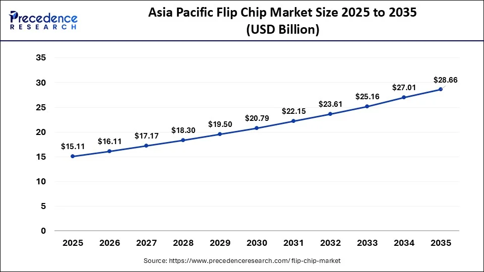
The Asia Pacific flip chip market size was valued at USD 15.11 billion in 2025 and is anticipated to reach around USD 28.66 billion by 2035, poised to grow at a CAGR of 6.61% from 2026 to 2035.

Asia Pacific led the market with the biggest market share of 37% in 2025. This dominance is propelled by China's semiconductor expansion efforts, alongside the emerging initiatives in countries like India, which collectively underscore the region's pivotal role in shaping the global semiconductor landscape. Its focus on the raw number of units rather than quality underscores its ambition to establish itself as a powerhouse in the semiconductor industry .
Chinese firms are strategically working to gain market share in foundational chip categories essential for various industries, including electric vehicles , consumer electronics, and household appliances. China's rapid expansion into the semiconductor design space is evident, with a multitude of firms multiplying in number and revenue. This growth reflects a widespread surge throughout the national semiconductor industry, positioning China to move up the electronics value chain and gain leverage in potential chip trade disputes.

India's semiconductor ambitions are also on the rise, as exemplified by HCL's joint venture with Taiwanese giant Foxconn to establish a semiconductor Outsourced Assembly and Testing (OSAT) unit. With Foxconn holding a 40 percent equity stake worth US$37.2 million, this collaboration signifies India's intent to strengthen its presence in the semiconductor ecosystem.
Recently, two semiconductor firms based in Karnataka, namely Saankhya Labs (a subsidiary of Tejas Network) and Sensesemi Technologies, were approved as beneficiaries under the Design-Linked Incentive (DLI) Scheme. This announcement was made by the Ministry of Electronics and Information Technology (MeitY) during the Digital India FutureLABS Summit 2024.
- In January 2024, India's cabinet endorsed an initial agreement between India and the European Union aimed at bolstering collaboration in the semiconductor domain. The Memorandum of Understanding (MoU) between India and the European Commission regarding Working Arrangements on semiconductor ecosystems, supply chains, and innovation was signed on November 21 of the previous year under the framework of the EU-India Trade and Technology Council (TTC).
Flip chip technology, initially developed in the 1960s, has emerged as a vital interconnect scheme facilitating connections between semiconductor dies or between dies and boards. The flip chip has evolved to enable various packaging solutions such as ball grid array (BGA) and double-sided molded ball grid array (DSMBGA), also referred to as controlled collapse chip connection (C4).
In DSMBGA packages, components are strategically positioned on both the top and bottom layers of the substrate, reducing package size and optimizing signal paths, which is particularly beneficial in minimizing power leakage in millimeter-wave circuits. Recent advancements in flip-chip technology, including innovations in wafer bumping, package substrates, flip-chip assembly, and underfill materials, have further enhanced its efficacy.
Flip chip bonding, also known as direct chip attach, involves attaching a semiconductor die, bond pad side down, to a substrate or carrier using conductive bumps on the die bond pads. This method offers several advantages over traditional interconnection processes, such as enabling higher I/O count by utilizing the entire die area for connections and improving device speed through shorter interconnection paths. Moreover, flip chip technology fosters direct and efficient bonding between chips and substrates, replacing conventional wire interconnections, thus streamlining manufacturing processes and enhancing overall performance.
- In March 2023, Jupiter Systems unveiled the Zavus Xtreme Pixel (XP) Flip Chip COB MicroLED, marking a significant advancement in display technology.
Advancing Semiconductor Packaging in North America
North America is the fastest-growing region during the forecast period. It is driven by the demand to secure supply chains, support AI/HPC needs, and enable next-gen technologies such as chiplets. The U.S. targets to prevent tampering and guarantees a reliable supply of chips for defense, automotive, and even critical infrastructure, decreasing reliance on offshore outsourcing.
Next-Generation Chip Integration in Europe
Europe shows a significant growth during the forecast period. It is driven by a strategic imperative to move from the position of research excellence to one of manufacturing sovereignty, along with industrial leadership. The COVID-19 pandemic, as well as shipping disruptions, highlighted Europe's high reliance on foreign semiconductor suppliers, mainly in Asia. This created severe supply shortages, notably in the European automotive industry.
Flip Chip in the Consumer Electronics Market in Latin America
Latin America shows a notable growth during the forecast period. This is due to the surging need for high-performance, compact, and energy-efficient consumer electronics, which include smartphones, IoT devices, and wearables. The proliferation of 5G, AI, and IoT devices in Latin America increases the demand for high-performance processors that utilize flip chip technology.
Flip Chip Market in MEA
MEA shows a rapid growth during the forecast period. It is driven by rapid digitalization, 5G deployment, along with increased adoption of automotive tech, consumer electronics, and AI in the region. The deployment of 5G infrastructure along with the increasing adoption of interconnected IoT devices, thus necessitate superior thermal as well as electrical performance, for which flip-chip technologies are preferred.
Flip Chip Market Companies
- Amkor Technology: Amkor Technology provides comprehensive, high-volume turnkey services, which include wafer bumping, assembly, and testing. They specialize in advanced technologies such as Copper Pillar, Flip Chip CSP (fcCSP), along with Flip-Stack for 3D packaging, thus catering to high-performance computing, automotive, and mobile markets.
- Intel Corporation: Intel Corporation is a vast player in the flip chip market, offering advanced packaging as well as assembly techniques via its Intel Foundry Services. Its portfolio focuses on high-performance, cost-effective, and even dense connectivity solutions mainly for AI, data centers, and high-performance computing.
- Fujitsu: Fujitsu focuses on advanced packaging technologies, wafer bumping services, and high-precision assembly for high-performance computing, consumer electronics, and networking.
Other Major Key Players
- Taiwan Semiconductor Manufacturing Company Limited
- Texas Instruments Incorporated
- SAMSUNG
- ASE Technology Holding Co., Ltd.
- Advanced Micro Devices, Inc.
- APPLE INC.
- Powertech Technology Inc.
Recent Developments
- In July 2023, Amkor announced the release of wire bond and flip chip packaging for TSMC's Advanced Low-k Processes.
- In September 2022, China emerged as the global leader in the production and sales of consumer electronics, showcasing its enhanced innovation capabilities and strengthened brand presence, according to the Ministry of Industry and Information Technology.
Segments Covered in the Report
By Packaging Technology
- 3D
- 2.5D
- 2.1D
By Bumping Technology
- Copper Pillar
- Tin-Lead Eutectic Solder
- Lead-Free Solder
- Gold Stud Bumping
By End-use
- Military and Defense
- Medical and Healthcare
- Industrial Sector
- Automotive
- Consumer Electronics
- Telecommunications
By Geography
- North America
- Europe
- Asia-Pacific
- Latin America
- Middle East and Africa
For inquiries regarding discounts, bulk purchases, or customization requests, please contact us at sales@precedenceresearch.com
Frequently Asked Questions
Tags
Ask For Sample
No cookie-cutter, only authentic analysis – take the 1st step to become a Precedence Research client
 Get a Sample
 Table Of Content


 sales@precedenceresearch.com
 +1 804-441-9344
 Schedule a Meeting