


Asia Pacific Semiconductor Glass Market Trends, Leading Companies, Company Revenue / Sales Performance, Manufacturing Yield, Fab Capacity, Export & Import Dynamics, Supply Chain Analysis, Competitive Landscape, and Growth Forecast
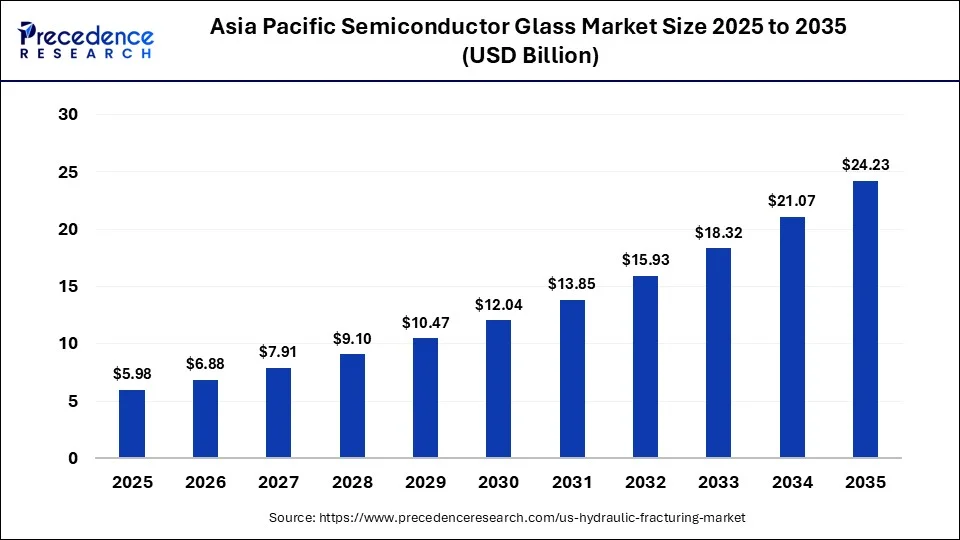
The Asia Pacific semiconductor glass market accounted for USD 6.88 billion in 2026 and is expected to grow at a CAGR of 15.02% from 2026 to 2035. The market is mainly driven by expanding AI and the advanced packaging transition, next-generation chip architectures, regional manufacturing dominance, and increasing electronics demand integration. The analysis was led by Laxmi Narayan, Senior Research Analyst, who brings experience in semiconductor and electronics market research. His analysis benefits semiconductor manufacturers, glass suppliers, electronics companies, and other stakeholders by supporting competitive analysis and enabling well-informed business decisions.
Source: https://www.precedenceresearch.com/asia-pacific-semiconductor-glass-market
 Get a Sample
 Table Of Content


Asia Pacific Semiconductor Glass Market Analysis, Demand, and Growth Rate Forecast 2035
The Asia Pacific semiconductor glass market is forecasted to expand from USD 6.88 billion in 2026 to USD 24.23 billion by 2035, growing at a CAGR of 15.02% from 2026 to 2035. The market is driven by increasing demand for advanced semiconductor manufacturing and expanding semiconductor fabrication facilities, along with electronics and chip manufacturing across the region. Laxmi Narayan, our Senior Research Analyst, has over 5 years of experience in the consumer goods industry. According to him, the ongoing investments in the semiconductor manufacturing infrastructure and the increasing adoption of advanced semiconductor technologies are creating future opportunities for semiconductor glass manufacturers and suppliers across Asia Pacific.
Key Takeaways
- By glass type, the Borosilicate Glass dominated the market with the largest market share of 36.20% in 2025.
- By glass type, the glass-core substrate materials segment is expected to have the fastest growth with a CAGR of 19.85% during the forecast period.
- By application, the glass wafer & panel carriers segment led the market with a 31.85% market share in 2025.
- By packaging architecture, the 2.5D packaging segment dominated the market with a 29.40% market share in 2025.
- By processing technology, the Precision Polished Glass segment held a major share of 28.65% in 2025.
- By end user, the foundries & IDMs segment led the market with the highest market share of 31.65% in 2025.
- The 2025 Asia Pacific market estimate of about USD 856 million can thus be treated as the broad regional TAM for this defined Asia Pacific semiconductor glass market.
- Samsung Electro-Mechanics established a glass-substrate pilot line targeting mass production from 2027 and announced an MOU with Sumitomo Chemical Group to create glass-core materials and a future production base.
- TOPPAN is building a pilot line in Japan for next-generation semiconductor packaging and glass components.
- SKC's Absolics also highlights another commercialization pathway, developing a dedicated semiconductor glass-substrate manufacturing operation in Georgia and continuing customer validation activities.
What was the Size of the Asia Pacific Semiconductor Glass Market in 2025?
The Asia Pacific semiconductor glass market is valued at approximately USD 856.24 million in 2025, occupying about 52% of the global semiconductor glass market. The regional outlook projects a 2026-2035 CAGR of approximately 14.25%, highlighting the regional cluster of semiconductor fabs, OSATs, advanced packaging facilities, glass-material suppliers, and electronics manufacturing. Available market evidence positions Asia Pacific at the center of semiconductor glass demand and shows strong regional adoption with separate estimates for glass interposers, glass carriers, and glass-core substrates.
Semiconductor glass encompasses specialty glass materials and processed glass substrates used directly in semiconductor manufacturing and advanced packaging, such as glass carriers, TGV substrates, glass interposers, glass-core substrates, quartz or fused-silica components, and selected glass materials for MEMS, sensors, and semiconductor processing. The glass itself functions as a semiconductor-processing or packaging material, excluding conventional glass-reinforced PCB laminates.
The market is shifting from the large-extent carrier and process-support applications toward higher-value glass-core, TGV, and advanced-packaging applications. AI accelerators, chiplets, high-bandwidth memory, co-packaged optics, advanced RF devices, and increasingly large package footprints help further generate requirements for low warpage, dimensional stability, fine-pitch vertical interconnects, and controlled thermal expansion. SEMI's 2026 research specifically identifies AI and HPC as major drivers for glass-core substrate development.
Concurrently, commercial adoption is mainly limited by glass brittleness, TGV processing cost, handling complexity, yield requirements, metallization compatibility, and the demand to qualify new packaging flows.
What Does The Market Trajectory Indicate?
The glass is shifting from being primarily a temporary carrier material toward becoming a functional component of the semiconductor package and ultimately driving the most important structural shift. This offers a larger value opportunity for suppliers capable of integrating glass chemistry, precision forming, polishing, through-formation, metallization compatibility, and panel-scale processing.
Analyst View for Market Size & Outlook
Asia Pacific will be positioned as the principal commercialization center because Japan, Taiwan, South Korea, and China integrate semiconductor manufacturing with advanced materials and packaging capabilities. The highest-value growth is likely to come from glass-core substrates and TGV-enabled interposers over conventional glass carriers alone. These further offer a major two-speed opportunity for the market, relatively established carrier demand alongside a much faster-emerging advanced-packaging opportunity.
Which Semiconductor Glass Type Accounts for the Largest Share?
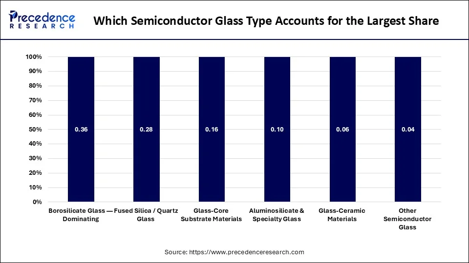
The borosilicate glass segment dominated the market with 36.20% market share in 2025. This dominance is mainly due to established semiconductor-processing and carrier applications, and broad availability and processing familiarity support its installed base. Followed by fused silica/quartz glass with 27.85% market share in 2025. The glass-core substrate materials segment is anticipated to have the fastest growth, with a CAGR of 19.85%, moving from development toward qualification and commercialization as package dimensions and interconnect densities increase. For instance, NEG developed large-format glass-core substrates, and TGV-processing approaches specifically for next-generation semiconductor packages.
Insights by Expert Analysts
The numeric data show a gradual transition from temporary carrier material toward becoming a functional component of the semiconductor package. By glass type, the borosilicate glass segment dominated the market, and the glass-core substrate materials segment is expected to have the fastest growth during the forecast period due to larger substrates and tighter dimensional control for AI/HPC package requirements.
How is Semiconductor Glass Being Used across the Packaging Ecosystem?
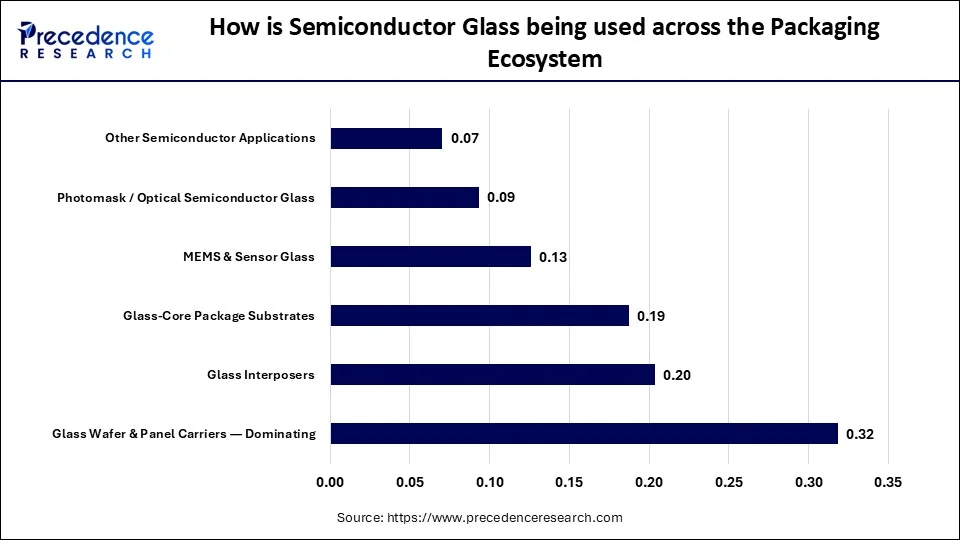
The glass wafer and panel carriers segment dominated the market, accounting for 31.85% market share in 2025. This application is fostered by increasing wafer-level and panel-level packaging flows. AGC supplies 300-mm wafers and approximately 500-mm-class panel carrier glass with high-flatness and high-smoothness specifications. The glass-core package substrates segment is anticipated to have the fastest growth, with a CAGR of 20.45%, because they address limitations emerging with larger chiplet packages and high-density AI/HPC architectures.
Insights by Expert Analysts
The glass wafer and panel carriers segment led the market with a 31.85% market share in 2025, followed by the glass interposers. This is because of the high requirement for flat temporary carrier substrates and the increasing demand for low-loss glass structures. Other applications like MEMS & sensor glass, photomask/optical semiconductor glass, and other semiconductor applications are also gaining traction in the future because of microfabrication, semiconductor patterning, and processing applications.
Which Semiconductor Packaging Architectures are Reporting the Strongest Demand?
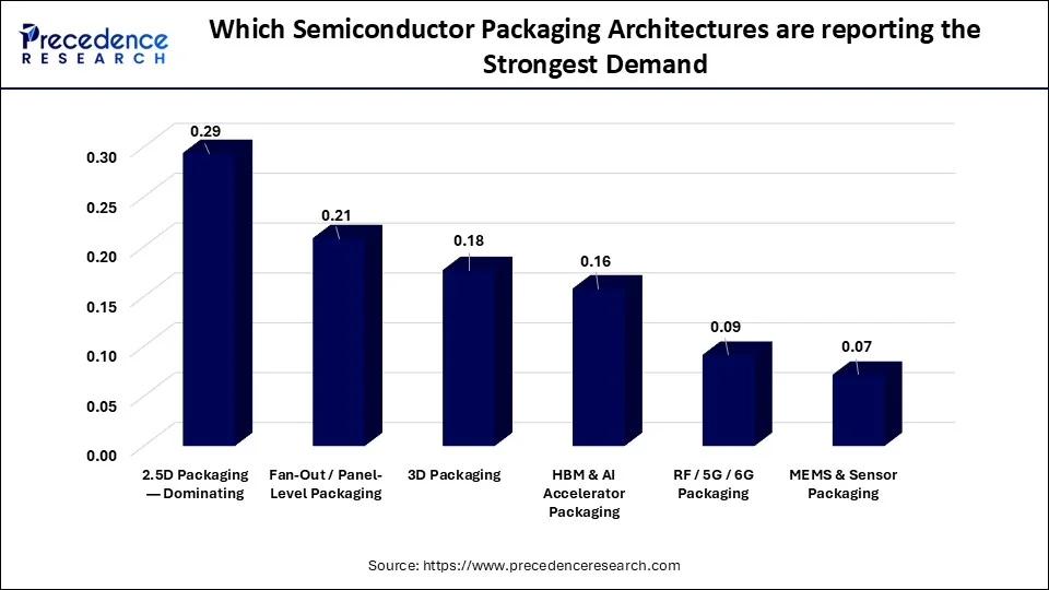
The semiconductor packaging architectures, especially the 2.5D packaging segment, held market dominance with a 29.40% market share and expected CAGR of 17.25%, mainly due to the broadest near-term applicability addressing high-density connections between logic and memory. Whereas the 3D packaging segment is expected to have the fastest growth during the forecast period, with a CAGR of 20.65% owing to its high-density interconnect requirements for the chiplet architectures and vertical integration.
Insights by Expert Analysts
The 2.5D packaging segment dominated the market, and HBM/AI-related and 3D packaging architectures also have the strongest expansion trajectory owing to AI packages that are forcing conventional package-size and interconnect challenges. SEMI's latest glass-core research specifically recognizes AI, HPC, advanced processors, and HBM-related packaging as important applications.
How Crucial Are Tgvs, Wafer Carriers and Panel Processing to Market Growth?
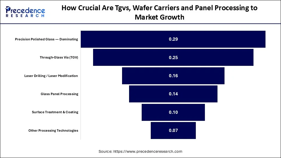
The precision-polished glass segment led the market with 28.65% market share in 2025, as it maintains its foundational technology because carrier and package applications depend significantly on flatness, thickness uniformity, and surface quality. Concurrently, the Through-Glass Via (TGV) segment is anticipated to have the fastest growth with a CAGR of 20.15% because it converts glass from a passive structural material into an electrically functional interconnect platform. AGC supports TGV diameters from approximately 20–150 μm and wafer formats up to 300 mm, while NEG has developed large 515 × 510 mm TGV glass-core substrates.
Insights by Expert Analysts
The precision-polished glass segment remains essential for its high flatness and surface quality, while TGV technology is gaining traction by enabling advanced vertical interconnections and glass core packaging.
Which Semiconductor End Users Hold the Largest Purchasing Pools?
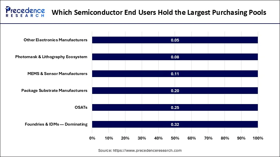
The foundries and IDMs led the market with 31.65% market share in 2025, mainly due to their heavy influence on qualification standards and determining packaging-process compatibility with advanced packaging integration and rising semiconductor process complexity. At the same time, OSATs segment is expected to have fastest growth with a CAGR of are expected to expand their purchasing share as advanced packaging becomes increasingly outsourced and packaging complexity rises.
Insights by Expert Analysts
This data highlights that semiconductor end users' largest purchasing pools are associated with the foundries and IDMs due to their process qualification and packaging compatibility. OSATs are expected to grow fastest as chiplet and HBM adoption accelerates.
What Are the Major Buyer Priorities and Adoption Barriers?
Semiconductor glass is a qualification-driven B2B material, highlighting that the price alone rarely determines supplier selection. Buyers also evaluate glass composition, CTE, flatness, TTV, surface roughness, mechanical strength, thermal stability, chemical resistance, via-processing compatibility, particle performance, and long-term supply reliability.
Various purchasing priorities include
- Dimensional stability: Essential for large package substrates.
- CTE matching: Glass must mitigate stress caused by thermal mismatch with silicon and other package materials.
- Surface quality: Flatness, TTV, and roughness directly influence downstream processing.
- TGV capability: Through diameter, pitch, aspect ratio, and metallization compatibility increasingly affect qualification.
- Yield: Defect density and breakage rates are essential because glass is more brittle than organic alternatives.
- Supply continuity: Semiconductor manufacturers prioritize qualified suppliers able to maintain consistent high-volume production.
- Customization: Customers significantly request specific CTE, thickness, and glass composition.
The commercial barrier is therefore not simply the cost of glass, but the total cost of qualified processing and integration.
Insights by Expert Analysts
Buyers prioritize dimensional stability, CTE matching, surface quality, TGV compatibility, yield, and supply reliability over price alone. Key barriers include qualification requirements, processing complexity, and the demand for consistent high-volume supply.
How are Leading Companies Positioning Themselves Across the Asia Pacific Semiconductor Glass Value Chain?
| Company | Market-Specific Capability / Activity | Strategic Significance |
| AGC | Glass carriers, TGV substrates, glass-core materials and semiconductor packaging materials | Broadest integration across glass material, carrier, and advanced-packaging applications |
| Nippon Electric Glass (NEG) | GC Core™, glass-core substrates, TGV substrates and semiconductor-supporting glass wafers | Strong positioning in large-format glass-core development |
| Samsung Electro-Mechanics | Glass package substrates and glass-core development | Bringing substrate manufacturing expertise into glass-core packages |
| TOPPAN | Glass-core FC-BGA substrates, glass panels and glass interposer development | Integrates glass processing with advanced package-substrate technologies |
| HOYA | Precision optical and specialty glass technologies | Relevant to high-purity semiconductor and optical applications |
| SCHOTT | Specialty and technical glass technologies | Strong materials engineering and semiconductor-related specialty glass capabilities |
| Corning | Advanced glass materials and glass-core substrate development | Technology position in high-performance glass and semiconductor packaging |
| SKC / Absolics | Commercialization of semiconductor glass substrates | Dedicated glass-substrate manufacturing approach for advanced packaging |
| DNP | Semiconductor packaging and glass-related advanced materials technologies | Position across precision processing and semiconductor packaging |
| Shin-Etsu Chemical | Semiconductor materials and high-purity specialty materials | Upstream semiconductor-material expertise |
The competitive landscape is developing across diversified areas including specialty glass production, carrier glass, TGV processing, glass-core substrates, package substrates, and advanced packaging. Among these, AGC clearly expanded its semiconductor portfolio around TGV glass substrates, carrier glass, and glass-core applications, while NEG shifted towards material development, including large-format TGV and glass-core sample availability.
Samsung Electro-Mechanics established a glass-substrate pilot line targeting mass production from 2027, and recently announced an MOU with Sumitomo Chemical Group to create glass-core materials and a future production base. Meanwhile, TOPPAN is building a pilot line in Japan for next-generation semiconductor packaging and glass components. SKC's Absolics also highlights another commercialization pathway, developing a dedicated semiconductor glass-substrate manufacturing operation in Georgia and continuing customer validation activities.
Insights by Expert Analysts
The competitive landscape is shifting from simply supplying specialty glass toward controlling the glass-to-package integration stack. Suppliers with capabilities spanning composition engineering, large-format forming, TGV development, surface treatment, and package qualification have greater strategic relevance. Asia Pacific companies also benefit from proximity to foundries, OSATs, and substrate manufacturers, with development and rapid qualification particularly important.
What is the Regional and Country-Level Structure of the Asia Pacific Market?
Asia Pacific's market is particularly concentrated in semiconductor manufacturing and advanced-packaging hubs rather than evenly distributed across the region.
How will China be considered the largest National Market?
China is considered the largest national market due to its unique combination of semiconductor manufacturing scale, packaging capacity, and domestic materials investment, thereby generating broad demand for semiconductor materials and packaging components. This supports the largest current demand base, and domestic semiconductor policies also support localization of critical materials and manufacturing technologies.
Why is India growing faster from a smaller base?
India's semiconductor ecosystem is largely shifting from predominantly electronics assembly toward semiconductor manufacturing, packaging, and supporting materials. Furthermore, its growth rate is primarily fostered by capacity creation and ecosystem formation rather than replacing demand. Government-backed ecosystem development, along with new investments, also drives a relatively high growth rate from a smaller installed base.
How will Japan emerge in the Market?
Japan is emerging as a significant player within the region, as Japan integrates semiconductor materials expertise with specialty glass manufacturing. NEG, AGC, and other Japanese companies are developing glass-core and TGV technologies, while Japanese substrate and semiconductor-material companies offer downstream integration opportunities.
Why is South Korea strategically important?
South Korea combines major memory manufacturers, advanced packaging activity, and package-substrate development. Samsung Electro-Mechanics is developing glass-core substrates and has established a pilot line, while the company demonstrates a Sumitomo Chemical collaboration shifting toward a broader glass-core ecosystem.
How will Taiwan Represent in the Market?
Taiwan's importance is connected to its foundry and advanced-packaging ecosystem. Demand from high-performance computing and AI packages creates an important downstream market for interposers, carriers, and next-generation glass substrates.
Insights by Expert Analysts
China currently provides the largest demand pool, Japan provides deep materials and precision-glass capabilities, South Korea combines memory and advanced substrate development, and Taiwan provides strong foundry-driven demand. India represents the most significant emerging opportunity from a low base. The region's competitive advantage therefore comes from the density of the entire semiconductor value chain, rather than from glass manufacturing alone.
What Does the Buyer Landscape Signal for Pricing, Procurement, and Commercialization?
Semiconductor glass procurement is primarily based on technical qualification following volume contracts, rather than spot purchasing.
- Pricing factors
- Glass composition and purity
- Surface roughness and flatness
- TGV diameter and pitch
- Laser-processing requirements
- Thickness and dimensional tolerance
- Wafer versus panel format
- Yield and defect density
- Customized CTE
- Volume and qualification status
A standard carrier glass product can therefore have a very different economic profile from a customized glass-core substrate with TGVs and package-ready surface treatment.
There are different adoption barriers, including:
- Glass fragility and handling: This leads to breakage and can negatively affect yield.
- Increased TGV cost: High-density through-processing adds equipment and process complexity.
- Growing metallization: Reliable copper or other conductor integration must be demonstrated.
- Qualification cycles: Semiconductor customers necessitate extensive reliability testing.
- Equipment compatibility: Existing packaging lines must be modified.
- Supply-chain concentration: Specialized glass formulations and processing capabilities remain a challenge.
What is The Important Opportunity Beyond the Current Semiconductor Glass Market?
A practical TAM/SAM/SOM framework expanded around advanced semiconductor packaging.
TAM
This is represented as a major market opportunity with a broader semiconductor-glass TAM, which encompasses:
- Carrier glass
- Quartz and fused-silica components
- TGV substrates
- Glass interposers
- Glass-core package substrates
- MEMS/sensor glass
- Semiconductor optical glass
The 2025 Asia Pacific market estimate of about USD 856 million can thus be treated as the broad regional TAM for this defined Asia Pacific semiconductor glass market.
SAM
This is another semiconductor-glass market with a more commercially focused SAM, and it would focus on:
- TGV substrates
- Glass interposers
- Glass-core substrates
- Advanced wafer/panel carriers
- AI/HPC packaging applications
These above-mentioned categories would represent approximately USD 516 million of the 2025 regional market when applying the integrated shares of the principal advanced-packaging categories.
SOM
At the same time, a realistic initial SOM for a new entrant should be based on qualification capacity over simply applying an arbitrary percentage to TAM. A supplier entering through one application, including TGV glass, carrier glass, or glass-core substrates, would need to qualify with a limited number of foundries, OSATs, or substrate manufacturers before expanding into volume programs
Overall, these opportunities would rapidly move from prototype qualification to repeatable high-yield production.
Which Fundamental Questions Should Companies Answer Before Entering Or Expanding?
Investment and capacity
- Which glass formats scale production first: wafer carriers, interposers, or glass-core substrates?
- What commercial scale is needed for competitive panel economics?
- Where should TGV processing capacity be located?
- Which regional country offers the best combination of semiconductor customers, skilled labor, and incentives?
Product strategy
- Should the company supply raw glass, processed carriers, or package-ready TGV substrates?
- Which CTE range should be focused on?
- What minimum TGV diameter and pitch are customers demanding?
- Can the same glass platform support both wafer and panel applicatins?
Commercialization
- Which foundries and OSATs should be considered for collaborative qualification?
- How long are typical qualification cycles?
- Which packaging architectures are addressable to volume adoption
- What yield threshold is necessary to displace silicon or organic alternatives?
Competitive positioning
- Is the differentiator glass composition, processing, cost, yield, or package integration?
- Is the supplier able to provide customization without sacrificing manufacturing economics?
- Is it able to provide both material and processing support?
- Which partnerships could accelerate customer qualification?
Insights by Expert Analysts
Successful market entry or expansion depends on investment and capacity for scalable glass formats that align with product strategies, customer demands, and applications. This further secures foundries and OSATs and achieves competitive costs and manufacturing.
Strategic Market Insights
The Asia Pacific semiconductor glass market is significantly shifting from supporting semiconductor processes to enabling next-generation package architectures. Carrier glass offers the established revenue base, but the strategic growth opportunity is rapidly concentrating in TGV glass, glass interposers, and glass-core substrates.
AI accelerators, HBM, chiplets, and larger package footprints are developing demands that conventional organic package materials increasingly struggle to address. Glass provides a combination of flatness, rigidity, dimensional stability, electrical insulation, and controllable CTE that makes it attractive for these applications. SEMI's recent industry work strengthens the connection between glass-core substrates and AI/HPC-driven advanced packaging.
The competitive landscape is relatively transforming toward integrated material-plus-processing platforms. AGC is integrating glass materials, carrier products, and TGV capabilities; NEG is producing large-format glass-core substrates; Samsung Electro-Mechanics is shifting toward glass package-substrate commercialization; and TOPPAN is emphasizing glass-core and glass-interposer technologies.
The decisive metrics will increasingly be yield for various buyers, TGV capability, large-format processing, CTE control, surface quality, and qualification reliability, over glass price alone. For suppliers, the strongest opportunity lies in becoming a qualified part of the semiconductor packaging process rather than remaining a commodity glass-material vendor.
Insights by Expert Analysts
The Asia Pacific semiconductor glass market is transforming with emerging growth opportunities such as TGV glass, glass interposers, and glass-core substrates, mainly driven by AI accelerators, HBM, chiplets, and advanced package footprints. Major suppliers that deliver higher yields, large-format processing, and meet customer qualification requirements strengthen the competitive positioning.
Our Experts
- The primary market research process was conducted by Laxmi Narayan, Senior Research Analyst, who also designed the methodology and did market segmentation, regional trend analysis, buyer intelligence, competitive assessment, and market forecasting, laying the foundation for the analytical part of the report.
- Aman Singh, Head of Research, has gathered and checked market data, semiconductor manufacturing trends, production capacity, company developments, technological advancements, and various other quantitative information sources, which were obtained independently, thereby increasing the quality of evidence supporting the calculations of the market values.
- Aditi Shivarkar, VP Research, has validated and refined the research material, verified facts, corrected inconsistencies, and completed the research document, making it accurate and to the point.
Asia Pacific Semiconductor Glass Market Segments Covered in This Report
By Glass Type
- Borosilicate Glass
- Fused Silica / Quartz Glass
- Glass-Core Substrate Materials
- Aluminosilicate & Specialty Glass
- Glass-Ceramic Materials
- Other Semiconductor Glass
By Application
- Glass Wafer & Panel Carriers
- Glass Interposers
- Glass-Core Package Substrates
- MEMS & Sensor Glass
- Photomask / Optical Semiconductor Glass
- Other Semiconductor Applications
By Packaging Architecture
- 2.5D Packaging
- Fan-Out / Panel-Level Packaging
- 3D Packaging
- HBM & AI Accelerator Packaging
- RF / 5G / 6G Packaging
- MEMS & Sensor Packaging
By Processing Technology
- Precision Polishing
- Through-Glass Via
- Laser Drilling / Laser Modification
- Glass Panel Processing
- Surface Treatment & Coating
- Other Processing Technologies
By End User
- Foundries & IDMs
- OSATs
- Package Substrate Manufacturers
- MEMS & Sensor Manufacturers
- Photomask & Lithography Ecosystem
- Other Electronics Manufacturers
By Country
- China
- Japan
- South Korea
- Taiwan
- India
- Singapore
- Malaysia
- Rest of Asia Pacific
For inquiries regarding discounts, bulk purchases, or customization requests, please contact us at sales@precedenceresearch.com
Frequently Asked Questions
Tags





Ask For Sample
No cookie-cutter, only authentic analysis – take the 1st step to become a Precedence Research client
 Get a Sample




 sales@precedenceresearch.com
 Schedule a Meeting