


Advanced Packaging Market Size, Key Companies, Company Market Share, Production Volume, Sales Performance, Export & Import Dynamics, Adoption Rates, Recycling Rate, Material Efficiency, and Demand Trends
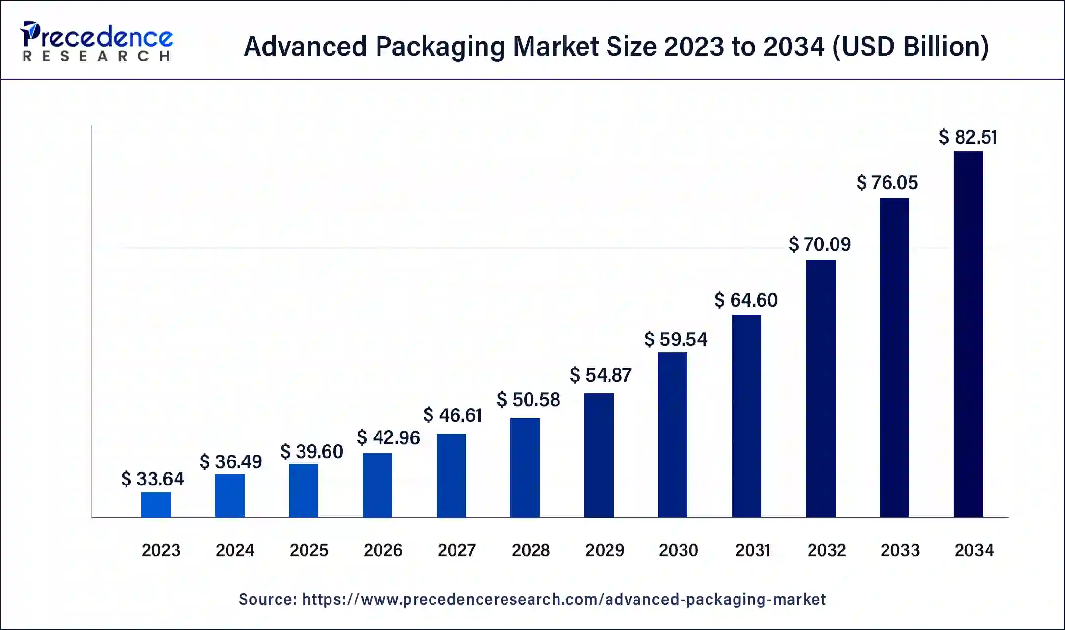
The global advanced packaging market was valued at USD 42.96 billion in 2026 and is projected to reach USD 88.63 billion by 2035, expanding at a CAGR of 8.39% from 2026 to 2035. Market growth is driven by rising demand for AI chips, high-performance computing, 5G, automotive electronics, and advanced semiconductor technologies. Increasing adoption of chiplet architectures, 2.5D/3D packaging, fan-out wafer-level packaging (FOWLP), and system-in-package (SiP) solutions is improving chip performance, power efficiency, and miniaturization across multiple industries.
Source: https://www.precedenceresearch.com/advanced-packaging-market
 Get a Sample
 Table Of Content


What is the Advanced Packaging Market Size?
The global advanced packaging market size is valued at USD 39.60 billion in 2025 and is predicted to increase from USD 42.96 billion in 2026 to approximately USD 88.63 billion by 2035, expanding at a CAGR of 8.39% from 2026 to 2035. The urge for advanced packaging is being driven by the demand to surpass the physical restrictions of regular chip production. By linking several smaller chips in a single package, it serves lower energy usage, higher processing energy, and minute creation factors that demand current technology.
Market Highlights
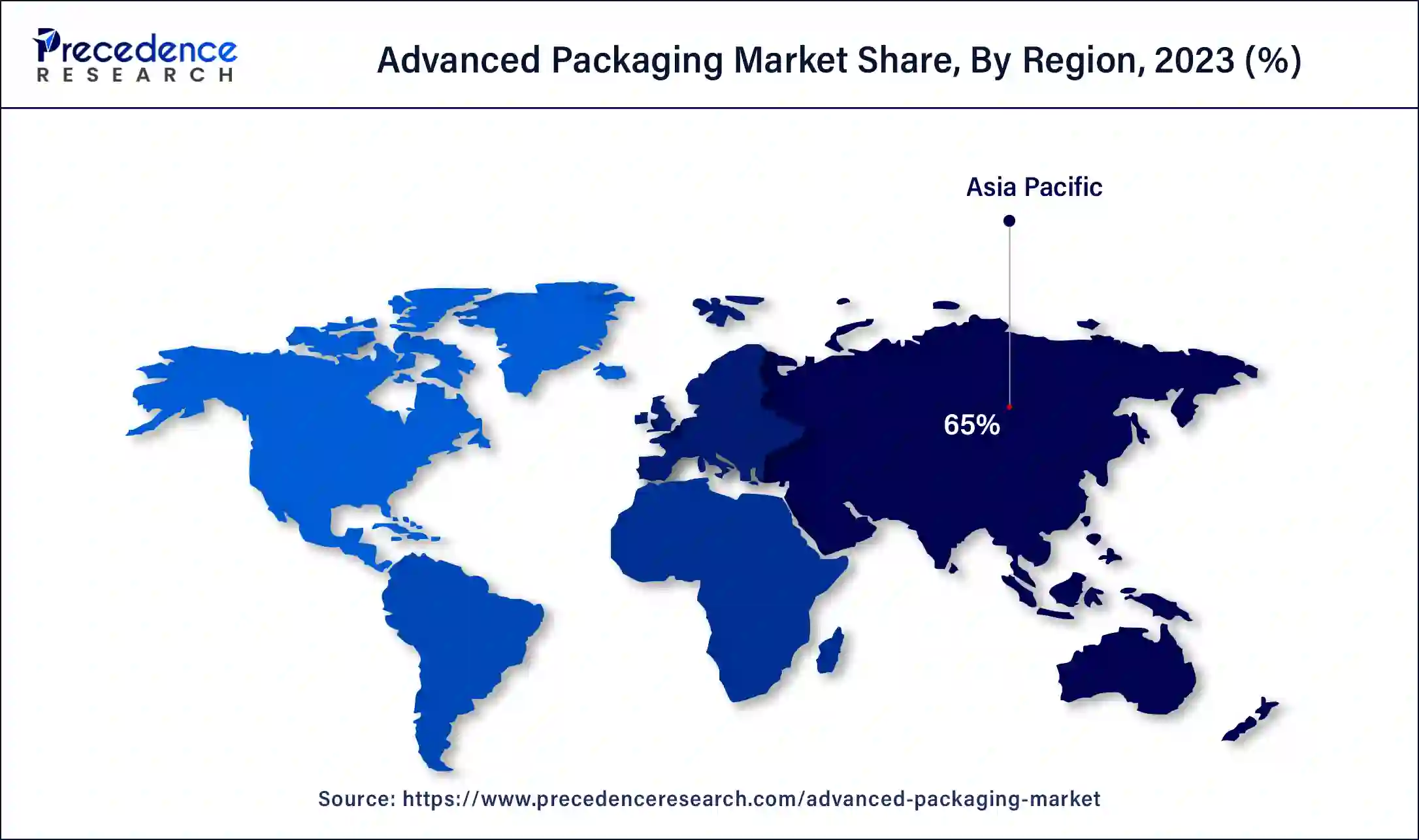
- Asia Pacific led the global market with the largest market share of 65% in 2025.
- North America is expected to expand at the fastest CAGR during the forecast period.
- By Type, the fan-out wafer-level packaging (FOWLP) segment has held the largest revenue share in 2025.
- By End-use, consumer electronics dominated the global market in 2025.
Market Overview
Advanced packaging encompasses innovative semiconductor manufacturing techniques that house, interconnect, and encapsulate multiple integrated circuits (ICs) and separate functional chiplets inside a single unified package. Core technologies involve 2.5D or 3D packaging, system-in-package, and fan-out wafer-level packaging to maximize connection density. These enclose a single die that leverages advanced approaches that use vertical stacking and ultra-fine pitch connections to bypass physical scaling limits. The market is further driven by the surging demand for AI accelerators, cloud data centers, and the shift toward chiplet designs that lower costs and improve thermal efficiency.
How will AI transform the Advanced Packaging Market?
Artificial Intelligence (AI) is transforming the global market by scaling performance where AI workloads require dense data transfer between logic and memory, which is solved by vertically stacking components and using high-bandwidth memory, owing to the rapid growth in chip stacking and glass core substrates. Machine learning and electronic design automation (EDA) flows shift manufacturing from basic simulation to learning-augmented co-design optimization. Splitting processors into smaller chiplets through advanced packaging prevents expensive single-node fabrication and optimizes overall efficiency.
Technological Advancement
Technological advancements in the advanced packaging market feature 3D packaging, chiplets, miniaturization, smart packaging, and system-in-package. The 3D packaging assembles multiple chips vertically, which proves an improvement in functionality even in a smaller space. The system-in-package merges multiple chips into a single substrate, supporting high-quality performance. The digital interface is a huge contribution to the advanced packaging market. The space for innovation in the market accelerates development on a large scale.
Miniaturization is an advanced packaging solution that allows the miniaturization of electronic appliances. The chiplets are small in size, specialized chips that can integrate intricate devices. The packaging industry is approaching advanced technologies to stimulate businesses. The advanced packaging system enables multiple devices to consist of semiconductor, electrical, and mechanical components. The system enables the packaging of a single electronic device. The combination of science and technology delivers several packaging solutions.
Advanced Packaging Market Growth Factors
The emergence in the advanced packaging technology has minimized the installation cost of ICs and enhances the output and efficiency of ICs and this factor is expected to drive the market growth. Also, with augmentation of IC in the automobiles, the demand for advanced packaging surged and this contributed positively towards the growth of the advanced packaging market. For instance, on 10th May 2021, Veeco Instruments Inc. announced that it has received an order for its AP300 Lithography System used in the production ramp of advanced packaging chips. This advanced packaging devices will be used to meet increasing demand for 5G system-on-a-chip, graphic processors (GPUs) and high performance computing applications. The AP300 systems were selected due to its industry-leading uptime and performance along with low ownership cost. This order indicates the fostering market demand for Veeco's lithography systems.
With the development in packaging technology, the functional density of large system-on-chip solutions has increased and this fosters the market growth. Moreover, the continuous research and developmental activities are performed in order to develop new and innovative packaging solutions and this will accelerate the growth of the advanced packaging market. Also, the rising demand for improving the performance of the electronic devices is estimated to fuel the growth of advanced packaging market. For instance, on 30th March 2021, YES (Yield Engineering Systems, Inc.), a leading manufacturer of process equipment for life sciences, semiconductor advanced packaging and AR/VR applications announced that it has received a large volume purchase order for the VertaCur XP from Taiwan-based OSAT Powertech Technology, Inc. The systems, which will be utilized for flip chip and wafer-level-packaging in high volume manufacturing, and it is expected to be delivered in the first half of 2021 to address growing production demands.
Furthermore, the surge in miniaturization of devices is assisting the embedded die packaging market gain renewed demand. Also, the heavy Government investment in developing semiconductor manufacturing plants specially in the developing nations are estimated to fuel the growth of market.
Market Outlook
- Industry Growth Overview: The advanced packaging market is growing, driven by rising demand for high-performance and contracted electronic devices. The increase of electric vehicles (EVs) and modern driver-assistance systems (ADAS) needs robust, high-performance semiconductor packages.
- Global Expansion: The advanced packaging market is experiencing global expansion due to the increasing requirement for high-performance, miniaturized electronics in various sectors such as consumer electronics, 5G, and AI. Asia-Pacific leads this growth, driven by growing manufacturing ecosystems in Taiwan, China, and South Korea.
- Major investors: Major investors are large integrated device manufacturers (IDMs) like Intel and Samsung, foundries such as TSMC, and outsourced semiconductor assembly and test (OSAT) companies such as ASE Group and Amkor Technology.
Trends in the Advanced Packaging Market
- Heterogeneous Implementation: Heterogeneous usage is transforming what is possible in semiconductor design by using various factors such as GPUs, CPUs, I/O, and memory that lie inside a single package. Such a strategy develops functionality and reduces power usage. By allowing various types of chips to be present in fixed integrated surroundings, it solves complicated design issues like growing data.
- High-Bandwidth Memory (HBM): Advanced packaging solutions are significant to the ideal usage of HBM, which serves unavoidable data transfer amounts for use in HPC and AI training. Wafer-level packaging (WLP) procedures ensure accurate alignment and strong interlinks, which allow the high-speed data to be complex for HBM's outcome.
- 3D ICs and the Chiplet Architectures: Chiplets serve the benefit of transformation, which enables designers to reuse the proven blocks and interchangeable elements that are personalized for applications. This not only lowers the growth amounts but also develops the time -to-market.
- Automation in High-Volume Production: Inventions in AI-driven process control and robotics allow for higher speed and accuracy in high-volume manufacturing (HVM). Such developments assist in making sure constant quality while lowering the waste, which is specifically crucial as the packaging has become more complicated.
- Thermal Management Innovations: Procedures such as using microfluidic cooling channels are directly present in the package, which use advanced thermal interface materials (TIMs) that assist engineers in showcasing heat more smoothly. Such solutions are necessary for managing the results of machines used in urgent surroundings, such as industrial and automotive uses.
Market Scope
| Report Highlights | Details |
| Market Size in 2025 | USD 39.60 Billion |
| Market Size in 2026 | USD 42.96 Billion |
| Market Size by 2035 | USD 88.63 Billion |
| Growth Rate from 2026 to 2035 | CAGR of 8.39% |
| Largest Market | Asia Pacific |
| Fastest Growing Market | North America |
| Base Year | 2025 |
| Forecast Period | 2026 to 2035 |
| Segments Covered | Type, End Use, and Region |
| Regions Covered | North America, Asia Pacific, Europe, Latin America, Middle East and Africa |
Market Dynamics
Driver
Maximizing Bandwidth through 3D Integration
The primary driver for the market is the physical limitation of conventional 2D Moore's Law scaling, which encourages the industry toward heterogeneous integration, chiplets, and 2.5D/3D IC architectures. Additionally, micro-systems integration, combining multiple functional dies into a single package, maximizes bandwidth, mitigates interconnect resistance, and improves thermal and power efficiencies.
Opportunity
Unlocking Growth in Next-Gen Microelectronics
A major market opportunity lies in the rapid expansion of automotive electronics, edge computing, 5G infrastructure, and AI accelerators that necessitate dense, low-latency multi-chip modules. Government-backed semiconductor incentive programs related to domestic manufacturing grants further catalyze regional expansions of advanced packaging lines and pave the way for new outsourced semiconductor assembly and test hubs.
Restraint
High Costs Block Small Firms
Despite its market potential, a major restraint for the market is the exceptionally high capital intensity and sophisticated technical complexity required for production. Issues like severe die shift, package warpage from thermal expansion mismatches, and stringent assembly tolerances hinder high-volume manufacturing yields and increase financial limitations for smaller market participants.
Segments Insights
Type Insights
How Fant-Out Wafer-Level Packaging (FOWLP) Segment Dominated the Advanced Packaging Market in 2025?
The Fan-out wafer-level packaging segment dominated the advanced packaging market in 2025 because it enables a greater number of I/O connections, apart from the physical limitations of the die. This is achieved by filling the die into a remanufactured wafer by using the further routing surfaces to stretch the I/O space, as the word “fan-out " assists in a higher density of links and delivers a developed electrical result.
The 2.5D/3D segment is expected to witness the fastest CAGR during the forecast period. It is driven by packaging, which enables various elements such as memory, processes, and sensors on a single package. Such closeness results in reduced interlink lengths, which points to developed lower latency and signal integrity. On the other hand, 3D packaging enables the compact design for a huge series of functionalities and elements, which makes them accessible for exceptionally complicated systems.
Application Insights
How the Consumer Electronics Segment Dominated the Advanced Packaging Market in 2025?
The consumer electronics packaging segment dominated the advanced packaging market in 2025, driven by economic and physical restrictions of regular transistor scaling, which allows several tailored chips to mix into a high-performance and single system. By transferring the complete concentration on creating specialized transistors while linking chips more smoothly, they have advanced packaging, which serves as the basic architecture for further generations of Artificial Intelligence (AI) and autonomous driving.
The automotive electronics segment is expected to witness the fastest CAGR during the forecast period. This is mainly due to developing complications of electronics systems, which are used in advanced driver-assistance systems (ADAS), vehicle-to-everything (V2X) communication, and infotainment, which is in higher demand for packaging solutions that can assist such complications. Advanced packaging enables developed heat dissipation, higher component densities, and enhanced electrical outcomes, as each one is important for automotive use.
Regional Insights
Asia Pacific Dominated the Market With a 71.88% Share in 2025
Asia Pacific dominated the mining equipment market by holding a major share of 71.88% in 2025 and is expected to expand at the fastest CAGR during the forecast period. Companies in this region are producing chips, both foundry and IDM, that serve a considerable amount of packaging services in the Asia Pacific region. The foundry operations of two companies, TSMC and Samsung, have the main packaging potential and are benefiting more from such demand for the chiplets to assist an AI capacity for their respective collaborators. Chiplets are also seeking direction into automotive, phones, and PCs, which are increasing the urge for chiplet potential for OSATS, which are giving feedback with foundries.
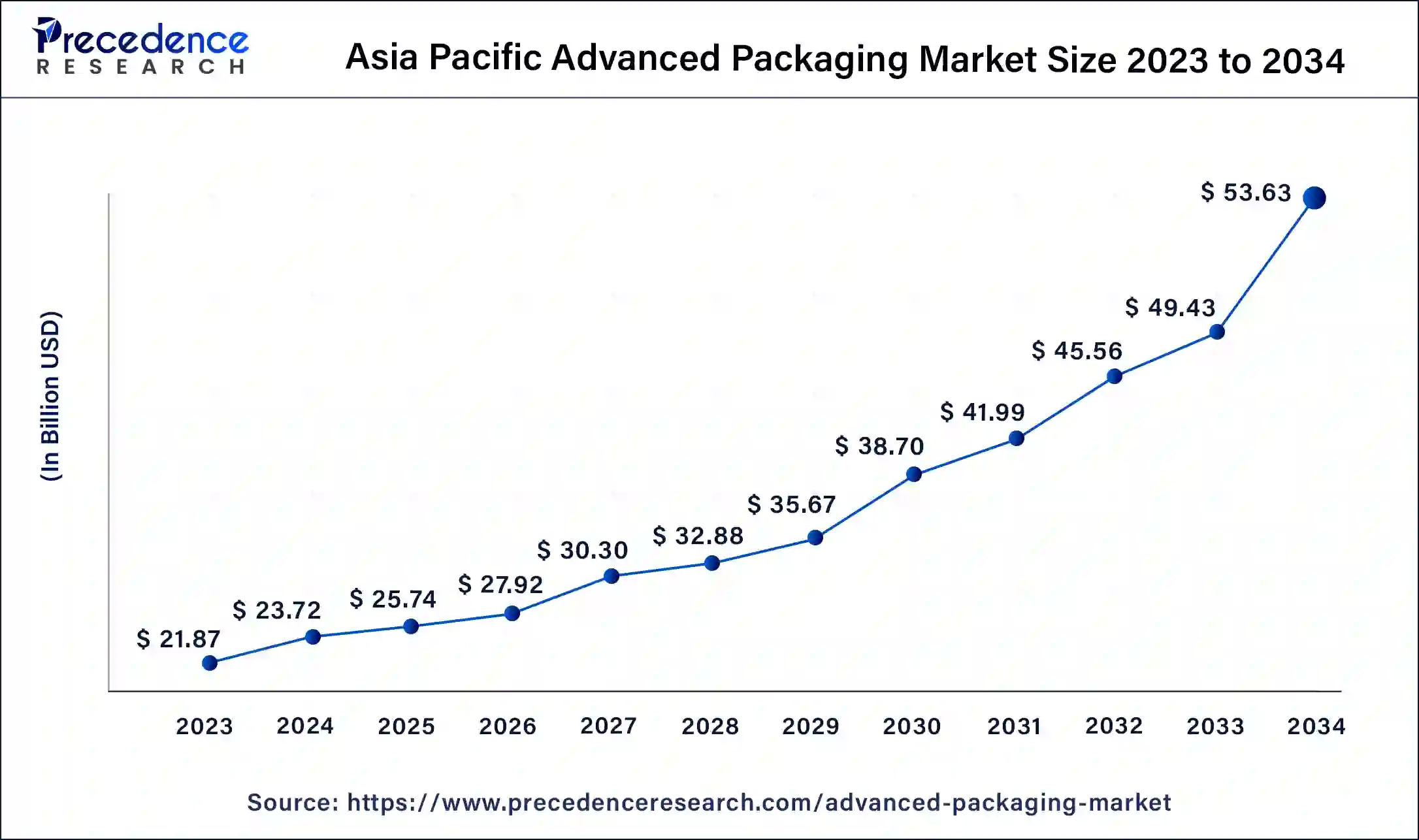
Asia Pacific dominates the advanced packaging market contributing a market share of more than 65% in 2025 and is expected to grow at a CAGR of 8.3% during the forecast period. It is because of the presence of major market players in this region and rapid growth in demand for semiconductors across various industry verticals such as automotive, consumer electronics, aerospace, defense and many others and the Government heavy investments in building semiconductor manufacturing plants specially in the developing countries such as India, China and South Korea. All these factors drive the growth of the Advanced Packaging Market. For instance, On 29th September 2021, Taiwan Semiconductor Manufacturing Co (TSMC) announced that it is developing new advanced packaging facilities in northern Taiwan. This advanced packaging fab in Chunan will be engaged in developing system on integrated chips (SoIC) technology.
Currently, Asia Pacific is dominating the advanced packaging market. Within the region, South Korea, Taiwan, and China hold the largest share of the market. The increased industries and excess demand for electronic gadgets require the largest rate of production of the packaging process. Another growth factor is that the production rate rises due to the several hubs of semiconductor manufacturing.
Trends of Advanced Packaging in India
China leads in the Asia Pacific market in terms of the fabrication side. Yield Engineering Systems, Inc. has started creating semiconductor equipment well in advance. The California company has revealed that it was the first to transport a main semiconductor production machine, named the Vero Therm Formic Acid Reflow System, to India for a worldwide chip manufacturer.
Why is North America Considered a Notably Developing Region?
North America held the second-largest market share of 8.64% in 2025 and is expected to grow at a CAGR in the upcoming period. This region is witnessing developing industrial growth, developing business needs, and technological developments. The organizations are funding advanced solutions to develop productivity, lower operational costs, and expand competitiveness.
Trends of Advanced Packaging in the United States
The U.S. is leading the North American market, driven by Texas City, which is a main semiconductor technology Centre that is specifically for advanced packaging that fits well with the parallel side of national security and economic competition. The Texas invention systems have a complete method across sectors like defense organizations, design centers, and the equipment companies, which are being assisted by a state rule infrastructure that is delivered by an enabling condition, as no other state has shown at such a range.
Europe: The Second-Largest Market
Europe held the second-largest market share of 15.73% in 2025 and is expected to grow at a CAGR in the upcoming period. The funding in competence centers and design stage's goal is to serve European consumers and companies to accurately access an electronic design automation (EDA) pilot and tools layers. Another main project is the “lab to fab” accelerator, which is an instrument to develop the shifting of technologies from official industry to research institutes that solve the technology space.
Trends of Advanced Packaging in Germany
Germany is the biggest microelectronics center in Europe. It has made an exceptional contribution to European semiconductor production, which means approximately 30% of wafer capacity. On the other hand, due to its higher share of value added in the industrial sector, they are excessively dependent on cutting-edge microelectronics. It invests about 4% directly and 15% indirectly in Germany's gross domestic product. The European Chips Act markets the well-developed action in a main technology present inside the European Union.
UK: Highly Skilled Talent Pool
The UK claims internationally renowned research institutions and a highly skilled talent pool specializing in modern materials and packaging enterprises. The UK government's National Semiconductor Strategy, a 20-year plan backed by significant spending, prioritizes the semiconductor subdivision, which drives the growth of the market.
Why is the Advanced Packaging Market Receiving Momentum in Latin America?
The market in Latin America is growing rapidly, which is supported by emerging production and usage hubs for electronics and information and communication technology (ICT), that counts the semiconductors which gives them energy. As the industry needs support within a web of segmented, complicated, and international supply chains, this one country will possibly have all the factors being urged for a complete semiconductor ecosystem.
Furthermore, Latin America is making an encouragement to grab the attention of particular spaces of the semiconductor supply chain, specifically in chip assembly, testing and packaging (ATP), and packaging (ATP), and likely that delivers the minerals if compulsory for semiconductor production.
Trends of Advanced Packaging in Brazil
Brazil is a major player in the Latin American advanced packaging market, driven by one of the most crucial developments for the national sector, which is the Brasil Semicon Program, which was launched in September 2024 under an official law 14,968/24, signed by President Luiz Inácio Lula da Silva.
Due to this newest legislation, the Brazilian Semiconductor Industry Association (Abisemi) has revealed RUSD24.8 billion in funds for research & development (R&D), for factory growth and production capacity expansion, with assistance by the year 2035.
How are the Opportunistic Rise of the Middle East and Africa in the Advanced Packaging Market?
The market in the Middle East and Africa is growing due to advanced electronics machines, which is mixed with the region's developed importance on infrastructure and development, which has triggered investment and interest in infrastructure and technologies.
This region totally depends on cutting-edge packaging technologies and imports of semiconductor components. Countries such as South Africa and Israel have grown as significant players, which have witnessed innovative and technological professionalism to drive this industry development.
Trends of Advanced Packaging in the UAE
The market in the UAE is experiencing steady growth due to the acceptance of artificial intelligence, which stretches across sectors. The industry is predicted to develop which application of autonomous technologies, learning models, and advanced analytics. Sectors such as automotive, healthcare, financial services, retail, and technology are funding in good-quality training datasets to develop the AI results.
South Africa Market Trends
South Africa made significant contributions to the market in the Middle East and Africa due to its highly developed food processing industry, wine export, and pharmaceutical sectors. Prominent developments in the country's market include the incorporation of antimicrobial liners in meat and poultry and breathable films for fresh produce. In recent times, packagers in the country have been seeking collaborations with European firms to develop innovative active and intelligent packaging.
Regulatory Guidelines for the Advanced Packaging Market
- U.S.: Authorized under the CHIPS for America research and development programs through NIST, this framework offers multi-billion-dollar investments targeting advanced packaging piloting facilities, power delivery, thermal management, and chiplet ecosystems to re-shore critical back-end capabilities.
- EU: Chips Act 2.0, managed through the European Commission, the EU framework leverages specialized pilot lines and state aid rules for First-of-a-Kind industrial deployment to secure back-end 3D advanced packaging, test, and assembly capacities across member states.
- India: Semiconductor Mission (ISM) 2.0 is highlighted in policy documents from the Ministry of Electronics and Information Technology (MeitY). This expanded phase strengthens domestic capabilities by scaling up fiscal support for outsourced semiconductor assembly and test and ATMP facilities.
Value Chain Analysis
- Raw Material Sourcing: It involves identifying and securing suppliers for specialized raw materials such as silicon interposers, photoresists, organic substrates, and epoxy molding compounds
Key Players: Veolia Environnement S.A. and Waste Management, Inc. - Material Processing and Conversion: It contributes a collection of manufacturing processes that integrate multiple semiconductor chips or components into compact, single, and high-performance electronic tools.
Key Players: SUEZ and Republic Services, Inc. - Recycling and Waste Management: It contributes processes such as developed mechanical and chemical recycling that break down plastics into their elementary components to create novel materials, including new fuels, plastics, and chemicals.
Key Players: Biffa Group Limited and MBA Polymers Inc.
Competitive Landscape
The advanced packaging market exhibits fragmentation to semi-consolidation with several regional companies alongside a few globally dominant firms. This market offers a low barrier to entry due to niche applications of innovations such as freshness indicators and antimicrobial film technologies, coupled with stiff price competition in mainstream products. Larger firms benefit from economies of scale and wider networks. Some of the key players include Amcor, Sealed Air, and Crown Holdings. There are new entrants like Infinite Cooling, which specializes in temperature-indicating labels.
Strategic developments include acquisitions by larger companies to obtain proprietary technologies like films and sensors, and collaborations with IoT companies to enhance connectivity. There have been many innovations in the market, such as AI-based quality control utilizing printed sensors, blockchain-compatible smart labels, and biodegradable active packaging. The entry barriers faced by new players include expensive material research and development, and an extensive regulatory process for food contact materials. The future forecast for the market is that the firms aspiring to be successful will need to implement digital technologies in a sustainable manner.
Top Vendors in the Advanced Packaging Market & Their Offerings
|
Company |
Headquarters |
Key Strengths |
Latest Info (2025) |
|
Amkor Technology Inc. |
Tempe, Arizona |
Diverse global manufacturing footprint |
In October 2025, Amkor Technology Breaks Ground on New Semiconductor Advanced Packaging and Test Campus in Arizona; Expands Investment to $7 Billion. |
|
ASE Technology Holding Co., Ltd. |
Kaohsiung, Taiwan |
Strong focus on innovation and advanced packaging |
In February 2025, ASE officially launched its fifth plant in Penang, which will significantly build on the company's strong packaging and testing capabilities. |
|
China Wafer Level CSP Co., Ltd. |
China |
High-volume manufacturing capabilities and strong relationships |
China Wafer Level CSP Co., Ltd. is a global leading supplier of 3DIC and TSV wafer-level chip size packaging and testing services. |
|
ChipMOS Technologies, Inc. |
Hsinchu, Taiwan |
Integrated outsourced semiconductor assembly and test services (OSAT) |
ChipMOS TECHNOLOGIES INC. is one of the world's largest semiconductor services companies, providing a full range of back-end testing services for liquid crystal display (LCD) |
|
FlipChip International LLC |
United States |
High-volume wafer-level packaging (WLP) |
developed flip chip packaging technology that uses a wafer-level packaging process to seek higher efficiency and cost-effectiveness. |
Recent Developments
- In May 2025, Saudi Arabia and Sidel signed a memorandum of understanding (MoU) to localize advanced packaging capabilities and strengthen industrial cooperation. This agreement focuses on the development of innovations in the advanced packaging market.
- In May 2025, Veeco announced over USD 35 million in advanced packaging lithography system orders from IDM & OSAT customers. The company is expecting growth with the financial investment and development.
- In April 2025, Siemens and Intel foundry advanced their collaboration to enable cutting-edge integrated circuits and advanced packaging solutions for 2D and 3D ICs. The strategic collaboration is leveraging the market presence globally.
Segments Covered in the Report
By Type
- Flip Chip CSP
- Flip-Chip Ball Grid Array
- Wafer Level CSP
- 5D/3D
- Fan Out WLP
- Others
By End-use
- Consumer Electronics
- Automotive
- Industrial
- Healthcare
- Aerospace & Defense
- Others
By Region
- North America
- Latin America
- Europe
- Asia-pacific
- Middle and East Africa
For inquiries regarding discounts, bulk purchases, or customization requests, please contact us at sales@precedenceresearch.com
Frequently Asked Questions
Tags





Ask For Sample
No cookie-cutter, only authentic analysis – take the 1st step to become a Precedence Research client
 Get a Sample




 sales@precedenceresearch.com
 Schedule a Meeting