What is the Electronic Design Automation Software Market Size?
The global electronic design automation software market size was calculated at USD 14.55 billion in 2025 and is predicted to increase from USD 15.89 billion in 2026 to approximately USD 34.71 billion by 2035, expanding at a CAGR of 9.08% from 2026 to 2035. The market for electronic design automation software is driven by rising semiconductor complexity, increasing adoption of AI tools, and expanding demand for advanced chip design solutions.
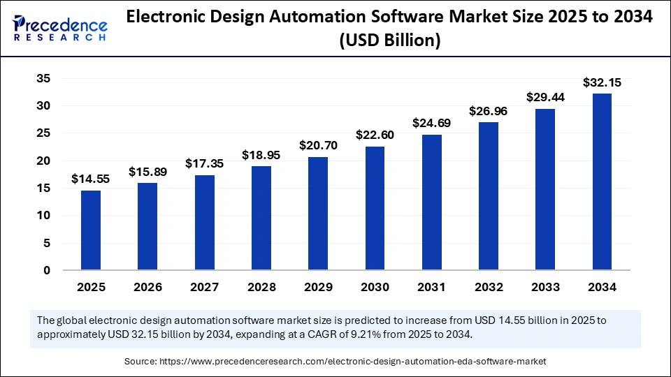
Market Highlights
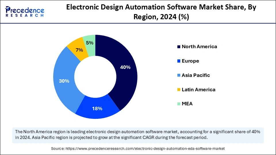
- North America led the electronic design automation software market with around 40% of the market share in 2025.
- The Asia Pacific is expected to expand at the highest CAGR between 2026 and 2035.
- By product type, the verification and sign-off segment held the major market share of 26% in 2025.
- By product type, the simulation & modeling (SPICE, EM, Thermal) segment is growing at the fastest rate from 2026 to 2035.
- By deployment model, the on-premise (perpetual / licensed) segment contributed the highest market share of 55% in 2025.
- By deployment model, the cloud-native SaaS / Pay-per-use segment is expanding at a strong CAGR between 2026 and 2035.
- By end-user industry, the semiconductor & fabless IC design houses segment held the largest market share of 45% in 2025.
- By end-user industry, the electronic systems OEMs segment is anticipated to grow at a high CAGR from 2026 to 2035.
- By application/use case, the ASIC/SoC design segment accounted for the biggest market share of 40% in 2025.
- By application/use case, the system-level & multi-discipline (SI/PI, thermal) segment is growing at a remarkable CAGR between 2026 and 2035.
- By sales channel/GTM, the direct enterprise sales segment captured approximately 55% of market share in 2025.
- By sales channel/GTM, the online / self-serve / app-store sales segment is expected to expand with the fastest CAGR from 2026 to 2035.
Building Resilience and Innovation Across Semiconductor Ecosystems
The key factors driving growth in the electronic design automation (EDA) software market are semiconductor complexity and growing demand for more efficient design verification tools. Electronic Design Automation (EDA) software comprises the tools and platforms used to design, simulate, verify, and implement electronic systems and integrated circuits (ICs), including front-end design (RTL, synthesis), physical design and layout, verification and sign-off, PCB design, simulation (electrical, electromagnetic, thermal), and related IP and automation tools that enable semiconductor, system-on-chip (SoC), PCB and multi-domain system development.
They allow engineers to maximize performance while decreasing errors and improving chip design cycles. The growth of AI, IoT, and automotive electronics is driving demand for new chip architectures. Furthermore, the continued adoption of system-on-chip (SoC) and new 3D IC technologies is driving the need for EDA tools, which are critical to next-generation semiconductor innovation.
AI and Data Analytics Revolutionizing Engineering Workflows
The role of artificial intelligence in the electronic design automation software market has moved beyond the pilot stage to a strategic application that is already enabling high-impact across chip development workflows. Vendors are embedding generative AI and agent-based AI to automate steps such as layout optimisation, verification, and workflow orchestration. For example, in June 2025, Siemens Digital Industries Softwares AI-enabled EDA suite was announced at the Design Automation Conference 2025, which provides secure generative AI flows, multi-agent capabilities, and custom integrations within semiconductor and PCB design tools.
At the same time, Synopsys is introducing AI-driven simulation, layout, and verification as strategic differentiators and accelerating workflows with GPUs and cloud-native delivery to serve the next-generation AI chip ecosystem. At the same time, the emergence of foundation model techniques in EDA implies an even more fundamental rewrite of how design data, scripts, and tool-flows are correlated and designed. Taken together as developments, EDA software is no longer simply automating design work steps it is becoming an intelligent contributor to semiconductor innovation.
Electronic Design Automation Software Market Outlook
- Industry Growth Overview: The Electronic Design Automation (EDA) software market is growing rapidly as complexity in semiconductor design continues to increase, and semiconductor companies push forward with innovation in AI, automotive, and high-performance computing. With the U.S. CHIPS and Science Act and the European Chips Act both incentivizing investment in advanced design infrastructure, there is continued demand for high-end EDA tools that optimize performance, minimize design timelines, and ensure designs are faithfully rendered at final fabrication.
- International Growth:Export-control policies are impacting international growth of EDA software: the US has put in additional license requirements on the export of design software to China as part of the advanced-chip supply chain. This highlights both the growth potential in new design regions and the burden of managing compliance across national jurisdictions for software companies.
- Research and Development: EDA tools are directly connected to the semiconductor design ecosystem across IC design, embedded systems, and multi-die modules. Government-directed semiconductor R&D projects will stimulate demand for tools, including tools developed by software companies that align themselves to new node innovations.
- Market Drivers:Increasing chip complexity (more transistors, multi-die packaging), growth in sectors such as automotive, AI accelerators, and IoT, as well as the drive for faster design cycles, all drive EDA software adoption. As chips become more tightly coupled together in end markets, the efficiency of design tools will become a competitive differentiator.
- Market Constraints:High costs of switching (tool-licensing, training, and flows), lack of talent in chip-design and verification, and regulatory risk (export/licensing regimes across major jurisdictions) all act as major constraints. Firms considering scaling up EDA tool adoption will need to account for these structural headwinds.
Market Scope
| Report Coverage | Details |
| Market Size in 2025 | USD 14.55 Billion |
| Market Size in 2026 | USD 15.89 Billion |
| Market Size by 2035 | USD 34.71 Billion |
| Market Growth Rate from 2026 to 2035 | CAGR of 9.08% |
| Dominating Region | North America |
| Fastest Growing Region | Asia Pacific |
| Base Year | 2025 |
| Forecast Period | 2026 to 2035 |
| Segments Covered | Product Type, Deployment Model, End-User Industry, Application/Use Case, Sales Channel/GTM, and Region |
| Regions Covered | North America, Europe, Asia-Pacific, Latin America, and Middle East & Africa |
Electronic Design Automation Software Market Segment Insights
Product Type Insights
The verification & sign-off segment leads the EDA software market, with a 26% share, because verification and sign-off tools are critical to ensuring designs are accurate for manufacturing. In semiconductor and chip design workflows, formal verification, equivalence checking, and timing or power sign-off tools are widely used to reduce functional errors and improve silicon yield, as they are highly valuable at scale for the production of high-performance integrated circuits.
The simulation & modeling segment is growing the fastest, again driven by increased demand for sophisticated circuit modeling using analogue, RF, and mixed-signal approaches. SPICE-based, electromagnetic, and thermal simulations can validate designs under realistic conditions, also driving approaches that will support innovation with AI accelerators, 5G, and in the automotive electronics space, where reliability and consistency are key.
The physical design & implementation segment remains critical to the market, as it provides tools for chip floor-planning, placement, and routing. Physical design tools optimize layout efficiency and power-performance trade-offs. In turn, physical design tools support chip and circuit designers in accommodating the increased transistor density and complex classifier architectures in nanoscale technologies, enabling manufacturability at scale and improving time to market.
Deployment Model Insights
The on-premises model segment led the electronic design automation software market with a 55% share in 2025, as organizations prefer EDA solutions with locally installed, perpetual licenses for performance and data security. In fact, large semiconductor and electronics firms prefer on-premises solutions because of the proprietary nature of chip designs, which require organizations to establish and enforce IP protection while handling high compute during design and verification cycles.
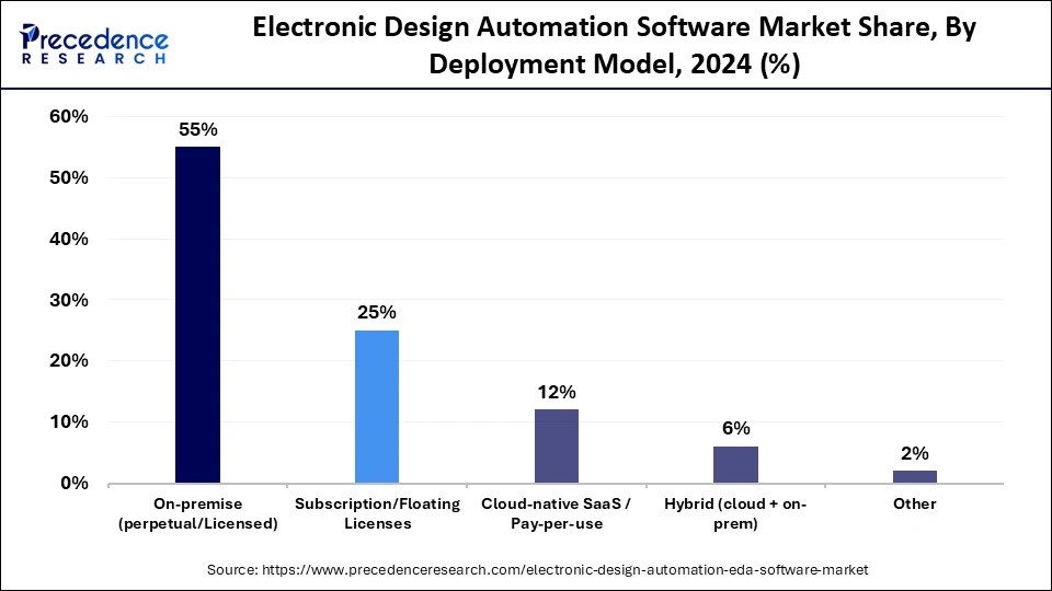
The cloud-native SaaS/pay-per-use segment was the fastest-growing in the electronic design automation software industry, driven by the shift to generative and collaborative design and the scalability of a cloud-based approach. Cloud-based EDA solutions on demand can be accessed by distributed design teams, solve the compute bottleneck, run workflows more efficiently, and reduce hardware costs, which are attractive to fabless engineering firms and mid-sized design firms seeking agility and cost advantages.
The subscription or floating license segment remains a notable market segment because organizations often seek flexibility in tool usage. This license allows EDA organizations to allocate EDA resources per project and/or team, enabling higher utilization of license products through dynamic capabilities and avoiding large or upfront expenditures for just one or two projects. This model may increase amongst companies balancing scale and control over their proprietary design environments.
End User Industry Insights
The semiconductor & fabless IC design houses segment led the market for electronic design automation software, with a 45% share, as chip architectures become more complex and demand for new applications in AI, IoT, and 5G expands. These organizations rely significantly on EDA tools for circuit design, verification, layout optimization, and to reduce the duration of tape-out and design-to-manufacturing time for the next generation of semiconductors.
The electronic systems OEMs segment is growing at the highest CAGR in the industry as device manufacturers are integrating more advanced chips and custom SoCs into consumer electronics, automotive systems, and industrial devices. OEMs are leveraging EDA solutions to improve product differentiation, power efficiency, and hardware-software co-design, as the lines between electronics, systems, and embedded intelligence become more blurred.
The foundries & integrated device manufacturers (IDMs) segment is seeing significant growth driven by advancing process technology and improved overall design manufacturability. Foundries and IDMs deploy EDA tools to check design rule compliance, optimize yield, and enhance process integration to minimize bridging across the design-to-fabrication distance and simultaneously optimize processes in the nanometre and heterogeneous integration domains.
Application / End-Use Insights
The ASIC/SoC design segment was the most popular with a 40% share in the electronic design automation software market, as it provides the infrastructure for advanced chip development across all industries. EDA tools in the ASIC/SoC Design segment help designers create custom logic, do timing verification, and integrate multi-core architectures. The growing demand for AI processors, automotive electronics, and 5G chipsets continues to drive global adoption of ASIC/SoC design workflows.
The system-level & multi-discipline (SI/PI, thermal) segment is growing the fastest in the electronic design automation software industry, driven by the increasing complexity of systems and cross-domain interactions in electronics. These tools analyze thermal and power integrity, as well as electromagnetic compatibility, enabling reliability and performance efficiency for very high-density chips packaged into systems or integrated across multiple-board systems.
The FPGA design & toolchains segment has seen notable market growth, as it is an important part of the EDA Ecosystem, enabling rapid prototyping and the development of reconfigurable hardware. It is common for engineers to use FPGA tools for verification or low-cost testing of orthopedic devices for new applications requiring flexibility, such as aerospace, defense, and industrial automation.
Sales Channel / GTM Insights
The direct enterprise sales segment is the largest in the electronic design automation software market, accounting for a 60% share because most major semiconductor companies and system designers prefer to engage directly with the vendor. The direct sales channel allows for customized licensing, free technical support, and integration with the in-house design infrastructure. The result is an easier deployment and maintenance process when large-scale design environments require sophisticated electronic design automation workflows.
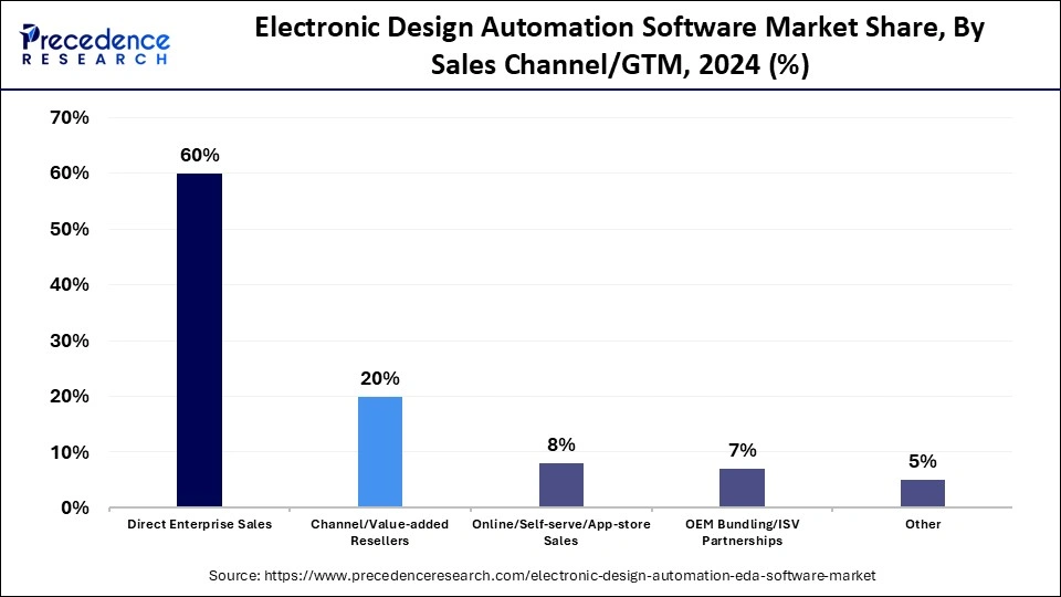
The online/self-serve/app-store sales channel is the fastest-growing segment of the market, driven by high demand for lightweight, cloud-based design tools. This segment enables startups and small engineering teams in smaller companies to access electronic design automation solutions immediately, providing a flexible, lower-cost entry for the next generation of electronics innovators.
The channel or value-added resellers segment remains important for enabling access to regional markets and small design houses. In these cases, the regional partners provide product education, localized learning experiences, and often bundled software to help the EDA vendor reach their customer base while addressing niche or localization-specific design challenges.
Regional Insights
How Big is the North America Electronic Design Automation Software Market Size?
The North America electronic design automation software market size was estimated at USD 5.82 billion in 2025 and is projected to reach approximately USD 14.10 billion by 2035, with a 9.25% CAGR from 2026 to 2035.
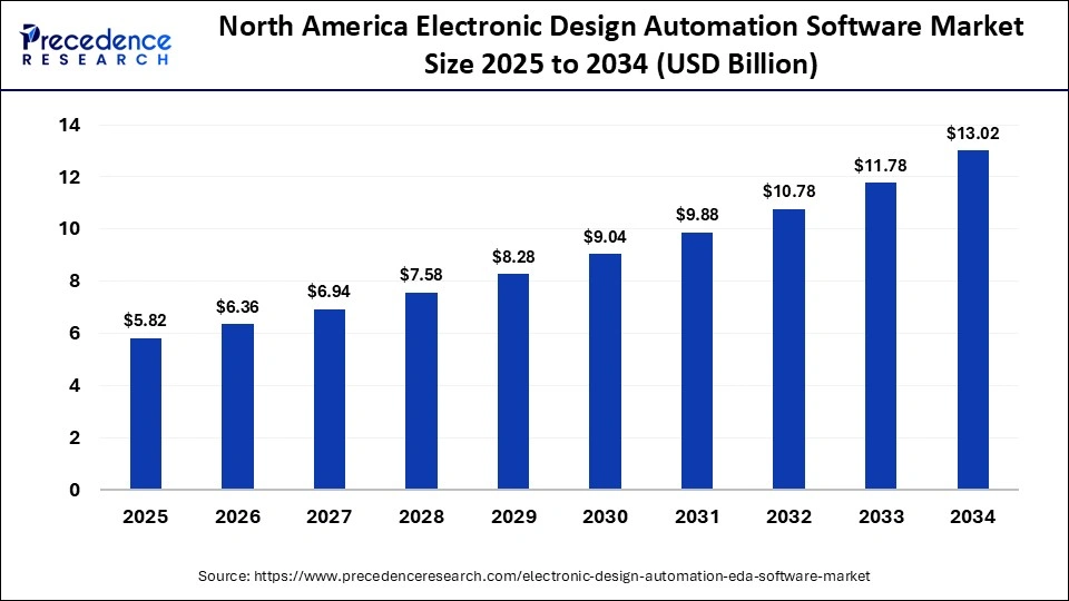
Why Is the Electronic Design Automation Software Ecosystem Anchored in North America?
The strength of North America is structural: with dense R&D clusters, the greatest concentration of EDA vendors, and significant public/private capital into chip design and fabs. Federal programs and industry R&D have increased demand for sophisticated design tools leading to platform upgrades (AI-enabled flows, system-level verification) and improved vendor revenues. Policy and manufacturing incentives have moved even more design work and collaboration with EDA, IDMs, and cloud/AI platform providers onshore, resulting in North America being the commercial market and standard-setting ecosystem for tool innovation.
What is the Size of the U.S. Electronic Design Automation Software Market?
The U.S. electronic design automation software market size was calculated at USD 4.25 billion in 2025 and is expected to reach nearly USD 10.38 billion in 2035, accelerating at a strong CAGR of 9.34% between 2026 and 2035.
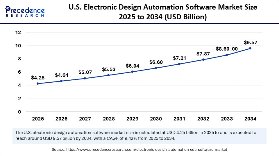
United States Electronic Design Automation Software Market Trend
The U.S. is the epicentre of global EDA: the global EDA leaders (Cadence, Synopsys, etc.) are headquartered or capitalized in the U.S. and well positioned to take advantage of CHIPS funding and tax credits that incentivize investments into domestic design and packaging. This builds cyclical demand that drives verification, integration of IP, and the AI-powered EDA tool chain relied upon by hyperscale and automotive and defence customers. Export controls and political policy have also consolidated high-end and commercial tool development in U.S.-based supply chains, further entrenching domestic vendor position and R&D clustering.
In November 2024, Keysight Technologies introduced a new Electronic Design Automation (EDA) software suite that leverages artificial intelligence to boost designer productivity, streamline workflows, and accelerate innovation across complex electronic system design processes.
What is the Asia Pacific Electronic Design Automation Software Market Size?
The Asia Pacific electronic design automation software market size is expected to be worth USD 10.63 billion by 2035, increasing from USD 4.37 billion by 2025, growing at a CAGR of 9.30% from 2026 to 2035.
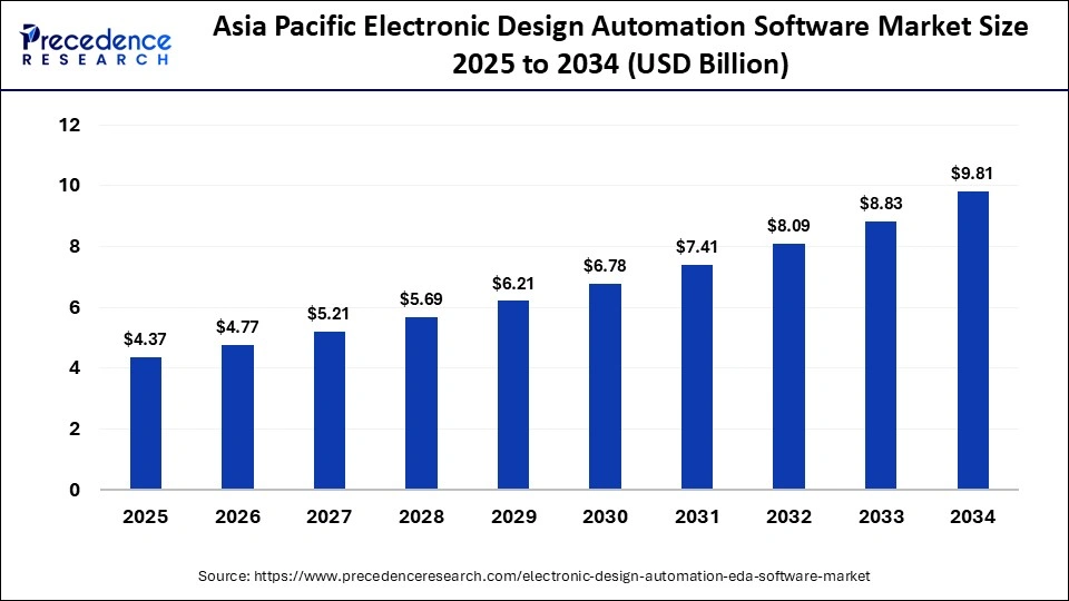
What accounts for Asia Pacific being the fastest developing EDA market?
Asia Pacific blends increasing demand for chip design with national industrial strategies: large consumer electronics , AI accelerators and automotive chips are leading to increased design headcount and custom IP development. Government and system integrators are accelerating investment into local a ecosystem which is driving up licensing of EDA flows for analog/mixed-signal, packaging co-design, and advanced verification. Market dynamics includes both adoptions of western EDA tools, along with fast expansion of local toolchains as supply-chain resilience has moved to a strategic priority.
India Electronic Design Automation Software Market Trend
The electronic system design industry in India is gaining momentum with solid policies and private sector investments. India is eying US$ 300 billion in electronics manufacturing and US$ 120 billion of electronics exports by FY26, signifying significant demand for much-needed EDA tools. In March, the Government of India, launched a 22,900 crore (US $2.68 billion) PLI scheme to incentivise the production in country to reduce dependency on imports.
Additionally, the Indian government allocated 8,803 crore (US $1.06 billion) for semiconductor and component manufacturing. Also, the need and thirst to get advanced EDA tools and local design automation capabilities is further energised by collaborations like Tata Consultancy Services and its partnership with Tata Electronics Pvt. Ltd., established to produce Indias first locally manufactured chipset.
China Electronic Design Automation Software Market Trend
Chinas market is unique due to heavy domestic demand for chip design, and regulatory pressures on export of foreign tools for chip design has triggered fast track development of home-grown tools and alternate supply paths. Chinese chip design firms remain major consumers of western EDA tools, but export control restrictions and government support, sparked rapid local innovation and adoption of home-grown EDA flows for mature and specialty nodes - Results in a bifurcated ecosystem of western tools for advanced nodes and fast-moving Chinese toolchains for the mature and specialty nodes.
- In September 2025, Chinese chip equipment supplier SiCarrier, a semiconductor equipment manufacturer supported by the Shenzhen municipal government collaborated with Huawei Technologies, and launched its proprietary electronic design automation (EDA) software.
What is the Europe Electronic Design Automation Software Market Size and Growth Rate?
The Europe electronic design automation software market size has grown strongly in recent years. It will grow from USD 2.62 billion in 2025 to USD 6.47 billion in 2035, expanding at a compound annual growth rate (CAGR) of 9.46% between 2026 and 2035.
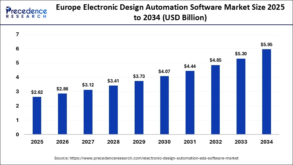
Why is Europe developing its Electronic Design Automation Software capabilities?
Europes strategy is motivated by a desire for policy-led semiconductor resilience and demand anticipated from automotive, industrial, and energy-efficient compute sectors. Public initiatives combined with the EU Chips Act have started cross-border investment in foundries, packaging, and design hubs, as well as motivated movement of workstreams toward localizing system-level design and verification. Strategic moves by global foundries and design houses to provide both capacity and design centres in Europe are shortening feedback loops between fabs and tool vendors, and facilitating the rapid adoption of AI-enabled toolchains and cloud-based EDA services across Europe.
Germany Electronic Design Automation Software Market Trend
Germany has a unique characteristics of scale in its industrial value chain, automotive semiconductor demand, and a major recent announcement of large investment in foundries and fabs, making it a natural candidate for driving EDA uptake in the areas of automotive-grade verification, high-reliability analog and power-management ICs, and advanced packaging . In addition, the engineering talent pool and cluster effects (universities, equipment suppliers, Tier-1 automotive OEMs) in Germany support accelerated cycle times for technical collaboration, and make Germany the key location of pilots in Europe for AI-driven verification flows and systems-level design toolchains.
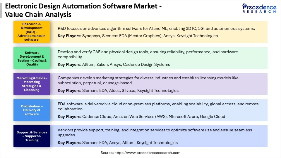
Electronic Design Automation Software Market Value Chain
Electronic Design Automation Software Market Companies
1. Synopsys Inc.
Corporate Information
- Headquarters: Sunnyvale, California, United States
- Year Founded: 1986
- Ownership Type: Publicly Traded (NASDAQ: SNPS)
History and Background
Synopsys, Inc. was founded in 1986 by Dr. Aart de Geus and a team of engineers specializing in digital design automation. Since its inception, Synopsys has become a global leader in Electronic Design Automation (EDA) software, semiconductor IP, and verification tools that power the design and production of advanced integrated circuits (ICs) and systems-on-chip (SoCs).
In the Electronic Design Automation (EDA) Software Market, Synopsys is recognized as one of the top two companies globally, providing comprehensive solutions for semiconductor design, verification, simulation, and manufacturing optimization. The companys platforms are essential for developing complex chips used in artificial intelligence, automotive electronics , and high-performance computing systems.
Key Milestones / Timeline
- 1986: Founded in Research Triangle Park, North Carolina, and later relocated to Silicon Valley
- 1992: Introduced Design Compiler, the industry first commercial logic synthesis tool
- 2012: Expanded into semiconductor IP through multiple acquisitions
- 2020: Released AI-powered DSO.ai platform for autonomous chip design optimization
- 2024: Launched Synopsys.ai suite integrating generative AI for design verification and timing closure
Business Overview
Synopsys develops software and hardware solutions that automate chip design, verification, and manufacturing. Its offerings include design synthesis tools, circuit simulation software , timing analysis, physical verification, and IP integration. The companys EDA solutions are used throughout the semiconductor design lifecycle, from concept to production, enabling faster time-to-market and reduced design complexity.
Business Segments / Divisions
- Design Automation
- Silicon IP
- Software Integrity Group (Application Security and Quality)
Geographic Presence
Synopsys operates in over 25 countries with major engineering centers in the United States, India, China, and Taiwan.
Key Offerings
- Synopsys Design Compiler for logic synthesis and design optimization
- PrimeTime for timing analysis and signoff
- Fusion Compiler for RTL-to-GDSII integrated physical design
- DSO.ai and Synopsys.ai AI-driven design automation platforms
- Verification Continuum for hardware and software co-verification
Financial Overview
Synopsys reports annual revenues exceeding $6.3 billion USD, driven by consistent growth in the semiconductor and EDA software markets.
Key Developments and Strategic Initiatives
- April 2023: Expanded Synopsys.ai capabilities for generative AI-based circuit optimization
- September 2023: Partnered with NVIDIA for AI-accelerated design workflows
- May 2024: Launched cloud-based EDA deployment suite to enhance scalability and collaboration
- January 2025: Introduced multi-node AI-driven verification environment for advanced chip designs
Partnerships & Collaborations
- Collaborations with semiconductor foundries such as TSMC, Samsung, and Intel for process technology enablement
- Alliances with cloud providers including Microsoft Azure and AWS for scalable EDA infrastructure
- Partnerships with automotive OEMs and AI chip startups for advanced SoC design
Product Launches / Innovations
- DSO.ai (Design Space Optimization AI) Platform (2020)
- Synopsys.ai Integrated AI Design Suite (2024)
- Cloud-native EDA collaboration tools (2025)
Technological Capabilities / R&D Focus
- Core technologies: AI-driven EDA, logic synthesis, timing analysis, verification automation, and design IP
- Research Infrastructure: R&D facilities in Silicon Valley, Bangalore, and Shanghai
- Innovation focus: AI-assisted automation, low-power design optimization, and multi-node manufacturing support
Competitive Positioning
- Strengths: Market leadership, deep foundry collaboration, and unmatched AI-driven EDA innovation
- Differentiators: Integration of machine learning into all stages of the chip design process
SWOT Analysis
- Strengths: Strong global market position, advanced AI integration, and broad IP portfolio
- Weaknesses: High software cost limits accessibility for smaller design firms
- Opportunities: Expansion into cloud-native EDA and AI hardware optimization
- Threats: Competitive pressure from Cadence and Siemens EDA in verification and simulation tools
Recent News and Updates
- March 2024: Synopsys announced partnership with Intel Foundry Services for AI chip design optimization
- July 2024: Released AI-assisted verification engine improving design turnaround by 30 percent
- January 2025: Unveiled next-gen Synopsys.ai system supporting fully autonomous design workflows
2. Cadence Design Systems Inc.
Corporate Information
- Headquarters: San Jose, California, United States
- Year Founded: 1988
- Ownership Type: Publicly Traded (NASDAQ: CDNS)
History and Background
Cadence Design Systems, Inc. was formed in 1988 through the merger of ECAD, Inc. and SDA Systems, creating one of the first comprehensive providers of Electronic Design Automation (EDA) software. Since its formation, Cadence has remained a key innovator in semiconductor design, simulation, and verification, driving the development of next-generation integrated circuits and system-level design platforms.
In the Electronic Design Automation (EDA) Software Market, Cadence is a leading competitor, providing end-to-end design and verification solutions for semiconductors, packaging, and printed circuit boards (PCBs). Its EDA tools support AI, 5G, automotive, and data center applications, enabling customers to accelerate chip development and achieve design closure with high precision.
Key Milestones / Timeline
- 1988: Established through merger of ECAD and SDA Systems
- 2000s: Expanded product suite to include analog and mixed-signal design
- 2019: Introduced AI-based Cerebrus Intelligent Chip Explorer for design optimization
- 2023: Acquired OpenEye Scientific to expand into computational design for life sciences
- 2024: Launched Cadence.ai platform integrating generative AI for semiconductor design automation
Business Overview
Cadence provides a complete EDA ecosystem that spans digital design, analog simulation, physical verification, packaging, and system analysis. Its software is used across the chip design lifecycle, helping engineers model, simulate, and verify complex integrated systems. Cadence is also expanding into AI-driven design automation and 3D-IC packaging.
Business Segments / Divisions
- Custom IC & PCB Design
- Digital & Signoff Systems
- Functional Verification
- System Design & Analysis
Geographic Presence
Cadence operates in over 25 countries, with major R&D centers in the United States, India, China, and the United Kingdom.
Key Offerings
- Cerebrus Intelligent Chip Explorer for AI-driven optimization of digital designs
- Virtuoso Platform for analog and mixed-signal IC design
- Innovus Implementation System for physical design and optimization
- Spectre Simulation Platform for analog verification
- Allegro System Design Platform for PCB layout and analysis
Financial Overview
Cadence Design Systems reports annual revenues of approximately $4.1 billion USD, supported by steady demand for EDA tools and growth in AI-enabled design automation.
Key Developments and Strategic Initiatives
- March 2023: Expanded use of AI in design workflows with Cerebrus platform enhancements
- September 2023: Partnered with TSMC and Samsung for 3nm and 2nm process design enablement
- May 2024: Introduced Cadence.ai, integrating machine learning across digital and analog flows
- January 2025: Announced cloud-based design collaboration platform for distributed engineering teams
Partnerships & Collaborations
- Collaborations with semiconductor foundries (TSMC, Samsung, Intel) for process certification
- Partnerships with cloud providers for EDA-as-a-Service delivery
- Alliances with automotive and 5G chipmakers for customized design workflows
Product Launches / Innovations
- Cadence.ai Platform (2024)
- Cerebrus AI-Enhanced Design Suite (2023)
- 3D-IC Packaging Flow with Integrity 3D-IC (2025)
Technological Capabilities / R&D Focus
- Core technologies: AI-based design automation, mixed-signal verification, and 3D-IC system packaging
- Research Infrastructure: Innovation centers in California, Bangalore, and Shanghai
- Innovation focus: Intelligent system design, machine learning-driven design closure, and energy-efficient simulation
Competitive Positioning
- Strengths: Deep analog and mixed-signal expertise, robust AI integration, and cloud scalability
- Differentiators: System-level co-design capabilities and AI-enabled optimization across design domains
SWOT Analysis
- Strengths: Strong EDA product ecosystem, AI adoption, and long-term industry partnerships
- Weaknesses: High pricing and licensing complexity for small firms
- Opportunities: Growth in 3D-IC design, cloud-based collaboration, and AI hardware
- Threats: Intense competition from Synopsys and Siemens EDA in signoff and verification
Recent News and Updates
- April 2024: Cadence introduced generative AI algorithms for power and performance optimization
- August 2024: Partnered with TSMC for 2nm and below node enablement on the Cadence.ai platform
- January 2025: Released new Cerebrus capabilities for multi-die system-on-chip (SoC) design optimization
Other Players in the Electronic Design Automation Software Market
- Siemens EDA (Mentor Graphics): Siemens EDA, formerly Mentor Graphics, is a global leader in electronic design automation software, offering solutions for IC design, verification, PCB layout, and system-level design. Its key tools, including Calibre, PADS, and Xpedition, are widely used for semiconductor design, DFM, and verification workflows.
- Ansys :Ansys provides simulation-driven EDA tools that integrate multiphysics analysis with chip design workflows. Its platforms, such as Ansys RedHawk-SC and Totem, enable power integrity, thermal analysis, and reliability verification for advanced IC and SoC design.
- Keysight Technologies: Keysight delivers EDA and electronic measurement software under its PathWave and ADS (Advanced Design System) suites. Its tools support high-frequency, RF, and mixed-signal design, as well as signal integrity and electromagnetic simulation.
- Altium: Altium specializes in PCB design software, including Altium Designer and Altium 365, offering integrated schematic capture, layout, and manufacturing tools. The company focuses on cloud-based collaboration and design efficiency for electronics engineers and OEMs.
- Zuken: Zuken provides software solutions for PCB and electrical design, including CR-8000 and E3.series. The companys EDA tools integrate schematic, layout, and mechanical co-design workflows, emphasizing enterprise-level data management and digital engineering.
- Silvaco: Silvaco offers TCAD, circuit simulation, and modeling software for semiconductor design and device fabrication. Its tools are used for process simulation, compact modeling, and parasitic extraction, serving both foundries and design houses.
- Empyrean Technology: Empyrean Technology develops analog and mixed-signal EDA tools covering circuit simulation, parasitic extraction, and timing analysis. The company focuses on delivering high-performance, cost-effective solutions tailored to emerging semiconductor markets.
- Aldec – Aldec provides FPGA design, simulation, and verification tools such as Riviera-PRO and Active-HDL. The company serves engineers developing digital designs for aerospace, defense, and communication systems with strong support for VHDL and Verilog standards.
- OneSpin Solutions: OneSpin offers formal verification tools and safety-critical design analysis solutions. The company specializes in equivalence checking and formal methods for ensuring design correctness and reliability in automotive and aerospace semiconductor applications.
- Apache Design (legacy technology/IP): Apache Design, now part of Ansys, pioneered power and thermal integrity analysis tools for semiconductor design. Its legacy technologies form the foundation of modern chip power management solutions integrated into the Ansys portfolio.
- Tanner EDA (Siemens): Tanner EDA, under Siemens EDA, provides software for analog, MEMS, and mixed-signal IC design. Its cost-efficient tools enable schematic capture, layout editing, and verification for smaller design teams and academic environments.
- Blue Pearl Software: Blue Pearl offers static verification and design automation tools for FPGA and ASIC design flows. Its software focuses on linting, clock-domain crossing (CDC) analysis, and design visualization to improve timing closure and functional reliability.
- Xpeedic Technology: Xpeedic provides EDA solutions for high-speed interconnect modeling, signal integrity, and electromagnetic simulation. The companys products are widely used for package, PCB, and system-level co-design in 5G and high-performance computing applications.
- Ansys Lumerical: Ansys Lumerical, part of the Ansys product suite, develops photonic simulation software for integrated optics, PICs (photonic integrated circuits), and optoelectronic design. Its tools bridge electronic and optical design workflows for next-generation photonics.
- ProteanTecs: ProteanTecs delivers EDA-adjacent analytics and design monitoring solutions for silicon lifecycle management. The companys software enables predictive analysis of chip performance, reliability, and degradation across manufacturing and field deployment.
- Cadence Design Systems: Cadence is a leading global EDA company providing comprehensive IC design, verification, and packaging software. Its Virtuoso, Allegro, and Spectre platforms support analog, digital, and mixed-signal design, alongside advanced AI-driven design automation and IP offerings.
- Third-Party IP Vendors (EDA-integrated): Several independent IP providers integrate with EDA workflows to offer reusable design blocks, verification IP, and libraries. These vendors complement EDA toolchains from Cadence, Synopsys, and Siemens by enabling faster, modular chip development.
- Efinix: Efinix develops FPGA solutions with design tools and workflows that complement traditional EDA environments. Its Quantum technology provides power-efficient, reconfigurable architectures supported by FPGA design automation software.
- Mentor/Tanner: Mentor/Tanner integrates analog and mixed-signal EDA tools within the Siemens EDA ecosystem. The combined offering targets MEMS and analog IC designers seeking streamlined schematic-to-layout workflows in cost-sensitive design environments.
Recent Developments
- In June 2025, Siemens Digital Industries Software introduced two new EDA solutions Innovator 3D IC and Calibre 3DStress to streamline heterogeneously integrated 2.5D/3D IC designs by addressing simulation, authoring, and reliability issues.(Source: https://news.siemens.com )
- In April 2025, Synopsys, Inc. and Intel Foundry announced a broad collaboration covering certified AI-driven digital/analog design flows and production-ready EDA for the 18A and 18A-P process nodes, including EMIB-T packaging support.(Source: https://www.newelectronics.co.uk )
- In June 2025, Samsung Foundry and Siemens expanded their cooperation: Siemens Calibre, Solido and Aprisa EDA tools now support Samsungs advanced processes from 14 nm down to 2 nm, alongside joint innovation in power integrity, silicon photonics and analog reliability.
Expert Opinion
According to analysts, the electronic design automation software market will grow steadily as increased chip complexity, system-level integration, and AI-assisted design will increase demand for advanced tool chains. Automotive, high-performance computing , and 5G communications applications will drive that growth, while new supply chain bottlenecks, IP security concerns, and a shortage of skilled verification engineers could constrain it.
Vendors focusing on cloud-native workflows, strong interoperability, and automated verification will capitalize on opportunities in chiplets, mixed-signal co-design, and ML-optimized physical implementation. Business models will migrate business to subscriptions and platform services, increasing performance and ROI expectations. Strategic M&A and targeted R&D will significantly differentiate global market leaders.
Electronic Design Automation Software MarketSegments Covered in the Report
By Product Type
- Verification & Sign-off
- Formal verification & equivalence checking
- Sign-off/timing / power/signal integrity tools
- IC Design / Front-end (RTL, Synthesis)
- RTL design & logic synthesis
- High-level synthesis (HLS)/ESL tools
- Physical Design & Implementation
- Placement & routing
- Floorplanning/optimization
- PCB Design & Board-level CAD
- PCB layout & routing
- PCB schematic capture
- Simulation & Modeling (SPICE, EM, Thermal)
- Circuit simulation, electromagnetic simulation
- Thermal, SI/PI simulation
- IP & Library Solutions
- Standard cell libraries, IP cores (memory, interface IP)
- DFT & Test
- Scan, ATPG, test compression, BIST tools
- EDA Services & Consultancy
- Integration, consulting, flow enablement
- Others/Miscellaneous
By Deployment Model
- On-premise (perpetual/licensed)
- Subscription/Floating licenses
- Cloud-native SaaS/Pay-per-use
- Hybrid (cloud+on-prem)
- Other
By End-User Industry
- Semiconductor & Fabless IC Design Houses
- Electronic Systems OEMs
- Foundries & IDM
- PCB & EMS providers
- Academic & Research
- Government/Defense/Aerospace
- Other
By Application/Use Case
- ASIC/SoC Design
- FPGA Design & Toolchains
- PCB & Board-level Design
- Package/Substrate Co-design
- System-level & Multi-discipline (SI/PI, thermal)
- MEMS & Sensor design
- Power & Thermal analysis
- Other
By Sales Channel/GTM
- Direct enterprise sales
- Channel/Value-added resellers
- Online/Self-serve/App-store sales
- OEM bundling/ISV partnerships
- Other
By Region
- North America
- Europe
- Asia-Pacific
- Latin America
- Middle East & Africa
For inquiries regarding discounts, bulk purchases, or customization requests, please contact us at sales@precedenceresearch.com
Frequently Asked Questions
Ask For Sample
No cookie-cutter, only authentic analysis – take the 1st step to become a Precedence Research client
 Get a Sample
 Table Of Content


 sales@precedenceresearch.com
 +1 804-441-9344
 Schedule a Meeting