Glass Interposers Market Size and Forecast 2025 to 2034
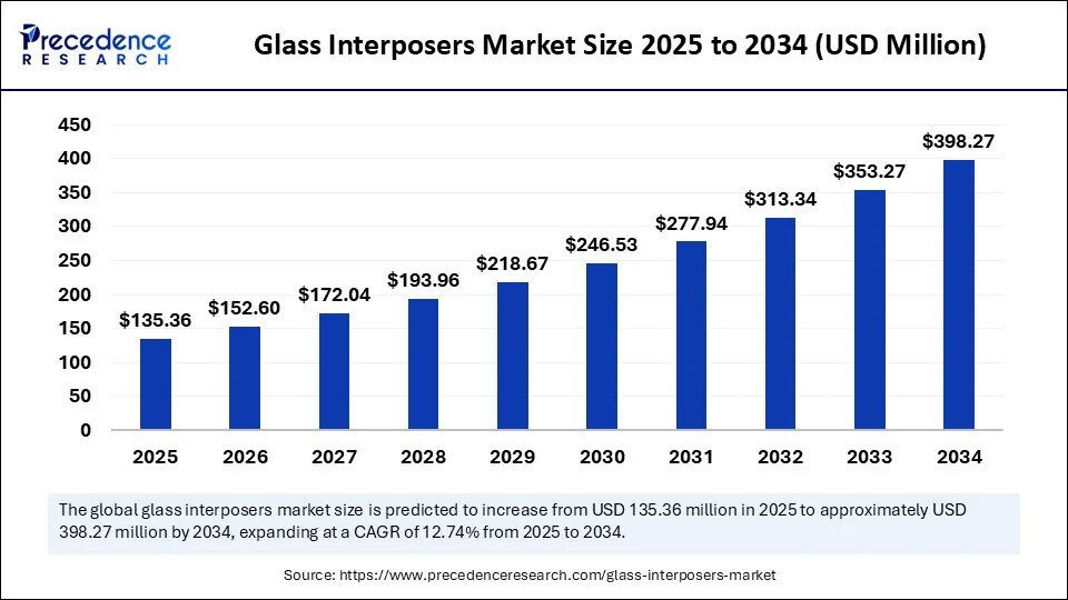
The global glass interposers market size was calculated at USD 120.06 million in 2024 and is predicted to increase from USD 135.36 million in 2025 to approximately USD 398.27 million by 2034, expanding at a CAGR of 12.74% from 2025 to 2034. The market's growth is being fuelled by rapid technological innovation, particularly the shift from traditional lighting systems to energy-efficient LEDs with customizable spectrum control.

Glass Interposers Market Key Takeaways
- In terms of revenue, the global interposers market was valued at USD 120.06 million in 2024.
- It is projected to reach USD 398.27 million by 2034.
- The market is expected to grow at a CAGR of 12.74% from 2025 to 2034.
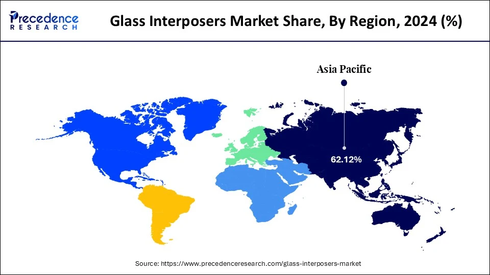
- Asia Pacific dominated the interposers market with the market share of 62.12% share in 2024 and is expected to grow at the fastest CAGR in the coming years.
- By product/type, the 2D glass interposers segment held the maximum revenue share of 55% in 2024.
- By product/type, the 3D glass interposers segment is expected to witness the fastest growth over the forecast period.
- By wafer size type, the 300 mm captured the largest revenue share of 60% in 2024.
- By wafer size type, the 200 mm segment is expected to witness the fastest growth over the forecast period.
- By substrate technology, the through-glass vias (TGVs) segment contributed the biggest market share of 70% in 2024.
- By substrate technology, the glass panel level packaging (PLP) segment is expected to witness the fastest growth over the forecast period.
- By application/packaging architecture, the 2.5D packaging segment generated the major market share of 65.34% in 2024.
- By application/packaging architecture, the fan-out packaging segment is expected to witness the fastest growth in the market over the forecast period.
How AI is Impacting the Glass Interposers Market?
Artificial Intelligence is reshaping the glass interposers market by optimizing design, manufacturing, and inspection processes. AI-driven simulation tools can rapidly analyze interposer layouts, predict thermal and electrical behavior, and recommend design improvements. This shortens development cycles while enhancing performance consistency. In manufacturing, AI-powered machine vision systems are improving TGV drilling precision and defect detection, minimizing yield losses. Predictive maintenance algorithms are also being used to keep fabrication equipment running at optimal efficiency. By integrating AI at multiple stages, manufacturers can scale production without compromising quality.
Asia Pacific Glass Interposers Market Size and Growth 2025 to 2034
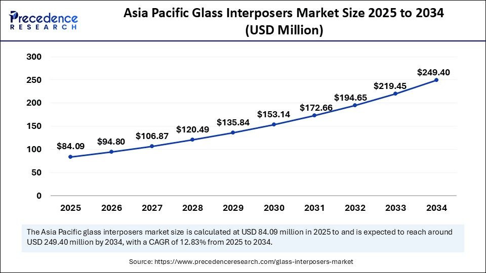
The Asia Pacific glass interposers market size is exhibited at USD 84.09 million in 2024 and is projected to be worth around USD 249.40 million by 2034, growing at a CAGR of 12.83% from 2025 to 2034.

Why Asia Pacific the Nerve Center of Glass Interposer Innovation?
Asia Pacific continues to dominate and is the fastest-growing region in the glass Interposers market, driven by its strong semiconductor manufacturing base and advanced electronics ecosystem. Countries like Japan, South Korea, Taiwan, and China host leading chip fabrication facilities and packaging houses that heavily rely on high-performance interposer technology. The rapid adoption of 5G, AI-enabled devices, and high-bandwidth memory modules in this region further boosts demand. Local supply chains benefit from a dense network of raw material suppliers, precision glass fabricators, and advanced lithography equipment providers. Government-backed R&D programs and strategic collaborations between academia and industry accelerate innovation in material properties and manufacturing processes. Moreover, Asia-Pacific's ability to produce at scale while maintaining cost efficiency makes it the preferred hub for high-volume production.

India is the dominant player in the Asia Pacific, and the glass interposers market is growing steadily, primarily fueled by the demand for advanced microelectronics and photonics-based applications. The country's research institutions are actively working on enhancing the thermal and electrical performance of glass substrates for next-gen devices. High-value applications such as aerospace, defense, and medical electronics are driving niche adoption . India-based startups and research labs are also exploring novel manufacturing methods like laser-assisted patterning and hybrid bonding. The presence of design houses collaborating with international manufacturing partners ensures a competitive role in the global supply chain. While the market is smaller in scale compared to Asia-Pacific, India's strength lies in innovation-led, specialized applications.
Bridging the Future of Microelectronics
The glass interposers market refers to the global industry revolving around the design, manufacture, and application of thin glass-based interposer substrates. These serve as electrically conductive bridges between integrated circuit components in advanced semiconductor packaging . Their advantages include excellent electrical insulation , thermal stability, dimensional precision, low dielectric loss, and superior ability to integrate ultra-dense interconnects, making them ideal for high-performance architectures like 2.5D and 3D chip stacking, fan-out packaging, 5G, AI accelerators, and miniaturized consumer electronics systems.
The glass interposers market is gaining momentum as the demand for advanced packaging in high-performance electronics accelerates. Glass interposers act as a crucial bridge between semiconductor dies and printed circuit boards, offering exceptional electrical performance and dimensional stability. Their superior thermal expansion properties, high signal integrity, and low warpage make them an attractive alternative to silicone interposers. Industries like high-speed computing, 5G, and advanced sensors are driving adoption. Glass interposers also enable more compact and lightweight designs, aligning with the miniaturization trend in electronics. As the semiconductor ecosystem evolves, glass interposers are emerging as a critical enabler of next-generation device performance.
Glass Interposers Market Key Trends
- Shift toward chiplet architectures and heterogeneous integration driving multi-die interposer demand.
- Miniaturization of devices requiring thinner, more precise, and thermally stable interposer materials.
- Growth of high-bandwidth memory (HBM) modules is increasing demand for high-density interconnects.
- Advances in through-glass via (TGV) technology improving signal integrity and reducing insertion loss.
- Adoption of panel-level processing for higher throughput and lower per-unit costs.
- Rising demand from 5G infrastructure and data center applications for low-loss, high-frequency performance.
Market Scope
| Report Coverage | Details |
| Market Size by 2034 | USD 398.27 Million |
| Market Size in 2025 | USD 135.36 Million |
| Market Size in 2024 | USD 120.06 Million |
| Market Growth Rate from 2025 to 2034 | CAGR of 12.74% |
| Dominating Region | Asia Pacific |
| Base Year | 2024 |
| Forecast Period | 2025 to 2034 |
| Segments Covered | Product / Type, Wafer Size, Substrate Technology, Application / Packaging Architecture, and Region |
| Regions Covered | North America, Europe, Asia-Pacific, Latin America, and Middle East & Africa |
Market Dynamics
Drivers
How Is the Chiplet Revolution Driving the Glass Interposers Market?
The strongest driver for the glass interposers market is the semiconductor industry's move toward chiplet-based architectures. This design approach allows multiple smaller dies to be interconnected on an interposer, improving yield, flexibility, and performance. Glass interposers excel here due to their ultra-low coefficient of thermal expansion (CTE) and exceptional dimensional stability. High-frequency applications like 5G radios, AI accelerators, and high-speed networking demand interposers that can handle tight signal tolerances. Additionally, the shift to heterogeneous integration is pushing packaging innovation, where glass offers a competitive edge over organic substrates. The synergy between system performance needs and material advantages is boosting demand.
Restraint
What Are the High Potential Barriers to Growth in the Glass Interposers Market?
Despite strong potential, the glass interposers market faces barriers that can slow adoption since the fabrication of through-glass vias at scale remains technically demanding, with tight tolerances and high precision requirements. Manufacturing yields can be lower than for traditional silicon or organic substrates, impacting cost competitiveness. Initial capital investment for production equipment and facilities is high, deterring smaller players. Additionally, design and process expertise for glass interposers is still concentrated in a limited number of companies. The complexity of integrating glass interposers into existing semiconductor supply chains adds another hurdle.
On the customer side, many device manufacturers remain cautious about switching from proven silicon-based interposers. Concerns about mechanical strength, handling, and long-term reliability must be addressed through rigorous qualification processes. Standardization is still evolving, making interoperability and multi-vendor sourcing more challenging. Cost parity with silicon interposers is not yet achieved for all applications, limiting uptake in price-sensitive markets. Any supply chain disruptions in specialty glass materials can further exacerbate risks. Overcoming these barriers will require industry-wide collaboration and sustained R&D investment.
Opportunity
How Are Data Centers and Devices Benefiting the Market for Glass Interposers?
Opportunities are high in the glass interposers market due to growth in technology verticals where these products can deliver unique advantages. Data centers processing massive AI and machine learning workloads require interposers with high signal integrity for rapid data throughput. 5G base stations and network infrastructure also present a growing market for low-loss, high-frequency capable interposers. In the consumer electronics sector, glass substrates can enable thinner, lighter devices without sacrificing performance. The automotive industry, especially in ADAS and EV power electronics, represents another untapped avenue. As more industries adopt high-performance computing , demand for glass interposers is set to rise.
Product / Type Insights
Why are 2D Glass Interposers Dominating the Glass Interposer Market?
The 2D glass interposers segment held a dominant presence in the market for glass interposers in 2024, due to their simpler design, mature manufacturing processes, and cost-effectiveness compared to more complex alternatives. They offer reliable electrical performance, low signal loss, and compatibility with existing semiconductor packaging lines. Their relatively straightforward fabrication makes them attractive for high-volume applications such as consumer electronics, networking devices, and optical modules. The scalability of 2D designs enables manufacturers to optimize for multiple performance ranges without significantly increasing cost. Additionally, their integration with high-density redistribution layers ensures robust interconnect density while maintaining thermal stability. These advantages make 2D glass interposers the go-to choice for industries prioritizing cost efficiency and reliability.
The dominance of 2D glass interpose is further reinforced by its extensive deployment in sectors such as telecommunications and automotive electronics . Their flat structure supports established assembly methods, reducing the need for specialized equipment. Manufacturers also benefit from shorter design devices. Continuous process improvements in photolithography and via formation have enhanced performance, closing the gap with more advanced 3D structures in certain applications. In addition, the lower defect rates and predictable yields of 2D glass interposers appeal to high-volume OEMs. This sustained adoption ensures their leadership position in the market.
The 3D glass interposers segment is set to become the fastest-growing in the glass interposers market, due to the increasing demand for high-bandwidth, multi-layer integration in AI, HPC, and advanced data processing systems. These interposers allow vertical stacking of logic and memory chips, reducing latency and improving energy efficiency. Their ability to support complex heterogeneous integration makes them highly suitable for next-generation chip architectures. As applications like AR/VR, 5G infrastructure, and autonomous systems evolve, the need for compact, high-performance interconnect solutions is accelerating adoption. The miniaturization trend in electronics is pushing the shift toward 3D interposers with improved density and performance per watt. Furthermore, advancements in glass via formation and bonding technologies are making 3D designs increasingly viable for commercial production.
This rapid growth is also driven by partnerships between semiconductor foundries, packaging houses, and material suppliers to scale up 3D glass interposer production. The design flexibility allows integration of multiple functional layers, enabling system-in-package (SiP) configurations. Although more complex and cost-intensive than 2D designs, their superior electrical and thermal characteristics make them indispensable for premium applications. Research in optical signal routing within 3D glass interposers is further expanding their potential. Additionally, AI workloads and edge computing deployments are heavily favoring architectures that benefit from 3D interposer performance gains. As economies of scale improve, cost barriers are expected to decline, accelerating adoption.
Wafer Size Insights
Why 300 mm is Dominating the Glass Interposer Market?
The 300 mm segment registered its dominance over the glass interposers market in 2024, due to its ability to support high-volume manufacturing with superior yield efficiency. Larger wafers allow for more interposers to be produced per batch, reducing overall cost per unit. This size is well aligned with modern semiconductor fabs and is compatible with advanced packaging technologies. Its adoption is widespread in consumer electronics, high-performance computing, and networking applications. The mature supply chain for 300 mm wafer processing ensures consistent quality and cost control. Additionally, economies of scale make it the preferred choice for large-scale production facilities.
The dominance of 300 mm wafers is also supported by the growing demand for advanced IC packaging in data centers and AI applications. This size enables the fabrication of interposers with higher complexity while maintaining consistent mechanical stability. It also allows manufacturers to optimize material utilization and reduce waste. Equipment for 300 mm wafer processing is well established, reducing the need for new capital investments. Furthermore, large wafer sizes align with industry trends toward higher integration and miniaturization without sacrificing electrical performance. As demand for high-performance devices increases, the 300 mm wafer segment is expected to maintain its leadership.
The 200 mm segment is predicted to witness significant growth in the glass interposers market over the forecast period, driven by its suitability for niche applications and specialty semiconductor manufacturing. Many mid-volume and prototype fabrication facilities rely on 200 mm equipment due to lower setup costs. This wafer size is often used in research environments and for specialized interposer designs in aerospace, defense, and medical electronics. The flexibility in handling smaller production runs without significant waste appeals to customized application markets. As industries explore heterogeneous integration for smaller device volumes, 200 mm wafers provide an economical entry point. Moreover, the retrofit of existing 200 mm fabs for glass interposer production is accelerating growth.
The growth of the 200 mm wafer market is also fueled by emerging economies establishing local semiconductor packaging capabilities. Smaller wafer sizes allow new players to enter the market without incurring massive infrastructure costs. Specialty applications requiring unique glass properties or geometries are often better suited for 200 mm processing. Additionally, with the rise of fab-lite models, the outsourcing of small-batch interposer manufacturing has increased demand for this size. Its role as a bridge between prototype development and larger-scale production adds to its appeal. Over time, improvements in process automation are expected to further boost adoption.
Substrate Technology Insights
Why Through-Glass Vias is Dominating the Glass Interposer Market?
The through-glass vias segment has become a dominant force in the glass interposers market, due to its unmatched electrical performance and high-density interconnected capabilities. TGV structures enable ultra-low signal loss and excellent thermal stability, critical for higher-speed and high-frequency applications. The ability to support fine-pitch routing makes them ideal for advanced IC packaging. TGV is widely used in RF devices, optical communication systems, and high-performance computing modules. Continuous process refinements have improved yield rates and reduced via defects, making the technology more cost-competitive. Additionally, TGV offers strong mechanical integrity, ensuring reliability in demanding environments.
The leadership of TGV tech in the market is reinforced by its compatibility with existing semiconductor manufacturing infrastructure. Its precision via formation techniques enables integration with both 2D and 3D architectures. Industries such as aerospace and defense value the long-term stability and signal integrity that TGV provides. Material innovations are further reducing the coefficient of thermal expansion mismatch, enhancing reliability. Moreover, its ability to facilitate vertical interconnections aligns perfectly with the miniaturization trend. As high-speed data applications expand, TGV's dominance is expected to remain strong.
The glass panel Level packaging segment has become the fastest growing in the glass interposers market, due to its promise of significant cost reductions through large-area processing. This method leverages glass panels instead of wafers, enabling higher throughput and better material utilization. The approach is attractive for applications requiring large-scale production without compromising precision. Advancements in panel handling equipment and patterning techniques are accelerating commercial adoption. As demand for low-cost, high-performance interposers grows, panel-level processing is emerging as a disruptive alternative. Additionally, its scalability makes it ideal for future generations of semiconductor packaging.
The rapid growth of panel-level glass packaging is supported by collaborative R&D between equipment makers and packaging houses. It offers a pathway to integrate high-density interconnects at reduced costs, which is crucial for mass-market applications. The method's compatibility with thin glass substrates also opens opportunities in flexible and wearable electronics. Although still in early adoption stages, pilot production lines are demonstrating promising yield rates. Furthermore, its potential to lower capital expenditure compared to wafer-based methods is attracting investment. With ongoing refinements, glass panel-level packaging is poised to gain significant market share.
Application/Packaging Architecture Insights
Why 2.5 packaging is Dominating the Glass Interposer Market?
The 2.5 packaging segment has become a dominant force in the glass interposers market, due to its balance of high performance and manageable manufacturing complexity. It enables integration of multiple dies on a single interposer, improving bandwidth and reducing latency. This architecture is widely used in graphics processors, network processors, and high-bandwidth memory modules. Its proven track record in commercial production makes it a safe choice for OEMs. Additionally, it supports heterogeneous integration without the thermal challenges often faced in full 3D architectures. The ability to reuse design elements across multiple product generations further enhances its appeal.
The dominance of 2.5D packaging is strengthened by its compatibility with both 2D and 3D interposers. It allows manufacturers to deliver improved performance without a complete overhaul of their production lines. Many semiconductor giants use 2.5D as a stepping stone toward full 3D integration. The architecture also offers good yields, reducing the risk associated with large-scale deployment. As AI and data center workloads expand, the demand for 2.5D-based interposers will continue to grow. Furthermore, incremental improvements in interconnect density and thermal management ensure its sustained leadership.
The fan-out packaging segment has become the fastest-growing in the glass interposers market, due to its ability to deliver high performance in ultra-thin form factors. It eliminates the need for an interposer substrate in certain designs, reducing thickness and weight. This makes it ideal for smartphones, wearables, and other space-constrained devices. Advances in glass-based fan-out methods are enabling better warpage control and improved electrical performance. The technology also supports high-density routing, making it competitive with more complex packaging solutions. Moreover, its compatibility with low-cost mass production techniques accelerates adoption.
The growth of fan-out packaging is driven by consumer demand for compact, high-performance devices. It allows manufacturers to pack more functionality into smaller footprints without compromising speed or efficiency. Glass substrates enhance mechanical stability, giving fan-out an additional advantage in reliability. The approach is being explored for high-frequency applications, expanding its market potential. Partnerships between OSATs (Outsourced Semiconductor Assembly and Test) and material suppliers are improving process maturity. As the technology scales, fan-out packaging is expected to become a mainstream choice for next-generation devices.
Glass Interposers Market– Value Chain Analysis
Raw Material Procurement
In the glass interposers value chain, raw material procurement is the foundational step that determines the overall quality and performance of the final product. The process typically begins with sourcing high-purity silica sand, which is refined and melted to produce ultra-clean glass substrates suitable for semiconductor packaging.
Key Players: Corning Incorporated, Plan Optik AG, and SCHOTT.
Testing and Quality Control
Quality control and testing in glass interposers focus on verifying key attributes such as electrical performance, mechanical strength, and optical clarity to guarantee both reliability and functionality. This process involves examining critical elements like through-glass vias (TGVs), redistribution layers (RDLs), and the interposer's overall structural integrity. Typical evaluations include electrical measurements for resistance, capacitance, and inductance, along with thermal cycling assessments and mechanical stress tests to ensure the interposer meets stringent performance standards.
Distribution to OEMs and Integrators
Glass-based interposer substrates are delivered to Original Equipment Manufacturers (OEMs) and Integrators through a specialized supply chain to produce glass interposers.
Glass Interposers Market Companies

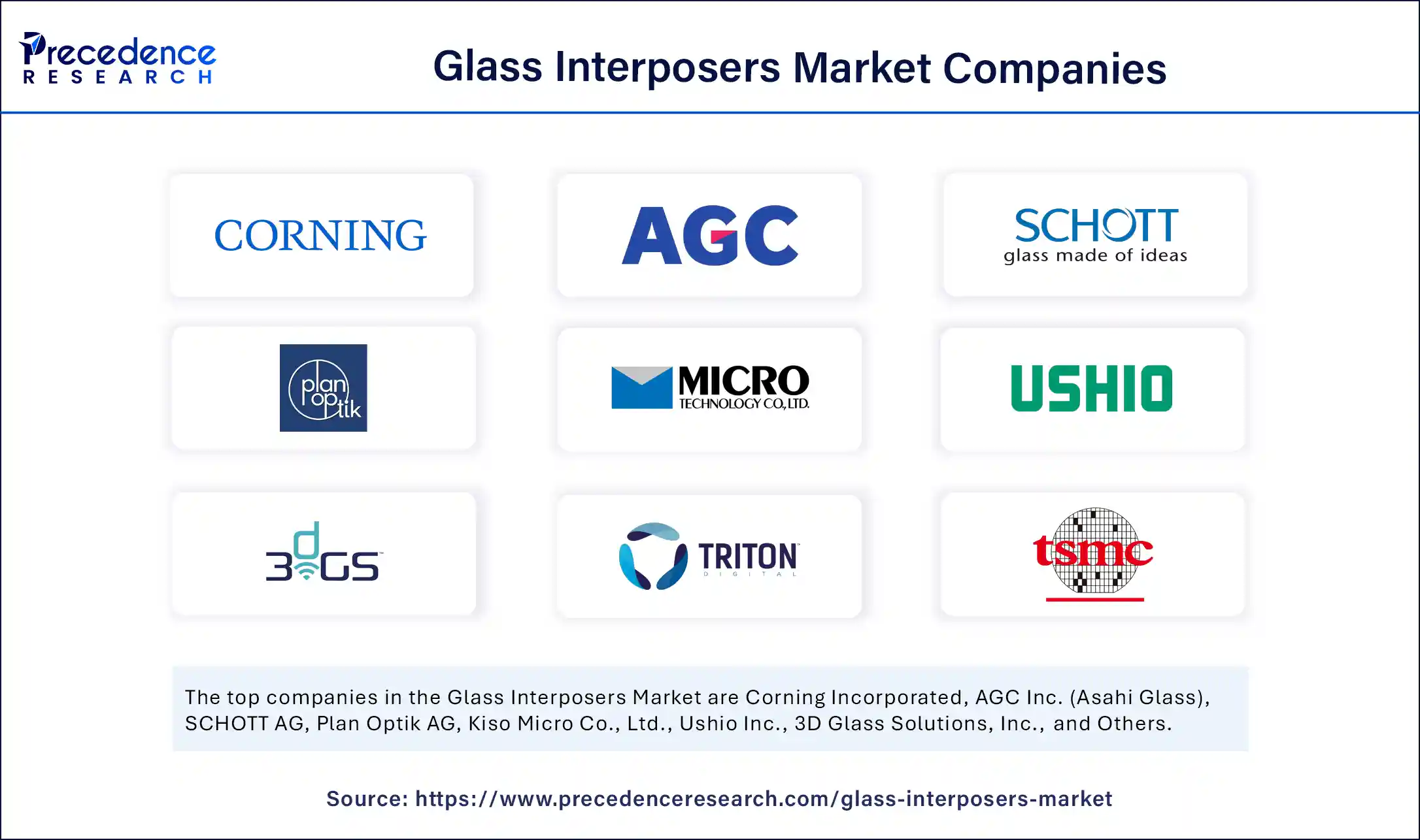
- Corning Incorporated
- AGC Inc. (Asahi Glass)
- SCHOTT AG
- Plan Optik AG
- Kiso Micro Co., Ltd.
- Ushio Inc.
- 3D Glass Solutions, Inc.
- Triton Microtechnologies, Inc.
- Taiwan Semiconductor Manufacturing Company (TSMC)
- Murata Manufacturing Co., Ltd.
- Dai Nippon Printing Co., Ltd.
- RENA (Glass interposer provider)
- Samtec Inc.
- Workshop of Photonics
- TECNISCO, LTD.
- Ohara Corporation
- Nippon Electric Glass (NEG)
- Entegris
Recent Developments
- In May 2025, according to reports, Samsung Electronics is working on a new glass substrate for advanced semiconductor packaging, with potential introduction targeted for 2028. In response to the growing demand for AI chips, the South Korean tech giant is exploring glass substrates as an alternative to silicon to lower manufacturing costs while enhancing overall performance. As part of its strategy to lead in this innovation, Samsung is said to be developing smaller panel prototypes, prioritizing performance improvements even at the expense of manufacturing efficiency.(Source: https://www.gadgets360.com )
Segments Covered in the Report
By Product / Type
- 2D Glass Interposers
- 2.5D Glass Interposers g
- 3D Glass Interposers
By Wafer Size
- < 200 mm
- 200 mm
- 300 mm
By Substrate Technology
- Through-Glass Vias (TGVs)
- Redistribution Layer (RDL) – First / Last
- Glass Panel Level Packaging (PLP)
By Application / Packaging Architecture
- 2.5D Packaging
- 3D Packaging
- Fan-Out Packaging
By Region
- Asia Pacific
- North America
- Europe
- Latin America
- Middle East & Africa
For inquiries regarding discounts, bulk purchases, or customization requests, please contact us at sales@precedenceresearch.com
Frequently Asked Questions
Ask For Sample
No cookie-cutter, only authentic analysis – take the 1st step to become a Precedence Research client
 Get a Sample
 Table Of Content


 sales@precedenceresearch.com
 +1 804-441-9344
 Schedule a Meeting