What is the 2D Materials Market Size?
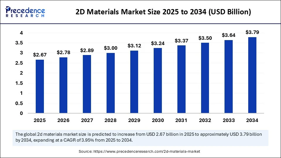
The global 2D materials market size is calculated at USD 2.67 billion in 2025 and is predicted to increase from USD 2.78 billion in 2026 to approximately USD 3.79 billion by 2034, expanding at a CAGR of 3.95% from 2025 to 2034. The market is driven by rising demand in electronics, energy storage, healthcare, and sustainable applications, supported by advanced R&D investments, government funding, and growing adoption across semiconductors, coatings, and optoelectronics.

2D Materials Market Key Takeaways
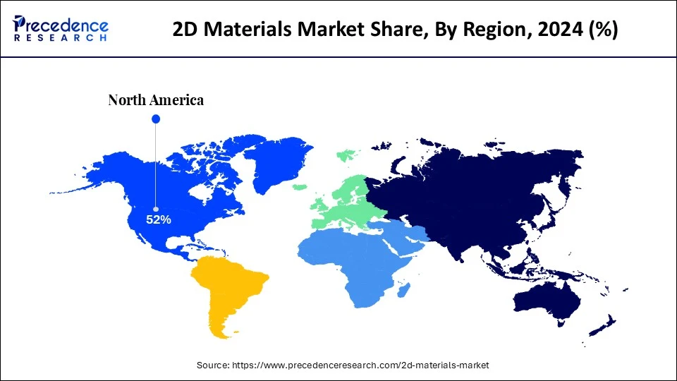
- North America dominated the global market with the largest share of 52% in 2024.
- Europe is anticipated to witness the fastest growth during the forecasted years.
- By material family, the TMDs (MoS?, WS?, WSe?, MoSe?) segment captured the biggest market share of 40% in 2024.
- By material family, the MXenes (Ti?C?T?, etc.) segment is anticipated to show considerable growth over the forecast period.
- By application, the electronics and optoelectronics segment contributed the highest market share of 33% in 2024.
- By application, the energy storage and conversion segment is anticipated to show considerable growth over the forecast period.
- By synthesis/format, the CVD/MOCVD/ALD wafers and films segment held the maximum market share of 44% in 2024.
- By synthesis/format, the solution-processed inks/dispersions segment is anticipated to show considerable growth over the forecast period.
- By end-user, the semiconductor and optoelectronic manufacturers segment generated the major market share of 31% in 2024.
- By end-user, the energy and storage OEMs segment is anticipated to show considerable growth over the forecast period.
Market Overview
The 2D materials market includes most disruptive directions in materials science, including atomically thin crystals of graphene , transition metal dichalcogenides (TMDs), hexagonal boron nitride (h-BN), MXenes, and black phosphorus. Their properties enable applications in next-generation electronics, optoelectronics , quantum computing , energy storage, coatings, membranes, and biomedical devices. The growing level of commercialization in graphene-based solutions, together with advances in scalable production of new 2D materials, makes the sector a key enabler to the semiconductor and clean energy sectors.
The 2D materials market is growing owing to the increased global demand for renewable energy technologies, electric mobility, and high-performance semiconductors. Their integration in hydrogen fuel cells, supercapacitors, lithium-sulfur batteries, and solar cells of the next generation enables the planet to move towards low-carbon energy systems. Additionally, adoption is further enhanced by the growing applications of transparent displays, flexible electronics , and barrier coatings within consumer electronics and aerospace markets.
How is AI Transforming the 2D Materials Market?
Artificial intelligence is changing the way of designing and fabricating 2D materials. Production AI applications, such as chemical vapor deposition (CVD) and molecular beam epitaxy (MBE), are also being automated to enable greater control of quality and homogeneity, and scale. It is becoming easier to find new 2D materials with application-tailored properties as computational models are increasingly being run using AI and machine learning algorithms that are becoming faster at predicting material properties. Very high conductivity, flexibility, and strength. Transition metal dichalcogenides (TMDs) and graphene have been more recently used in neuromorphic computing , quantum devices, and dense, low-power 3D integrated circuits.
2D Materials Market Outlook
- Industry Growth Overview: The 2D materials market is expected to grow rapidly from 2025 to 2034, fueled by demand for high-performance, miniaturized electronics and expanding uses in energy storage and biosensors. The growing use of graphene in advanced electronics and TMDs for next-generation semiconductors further drives market growth.
- Integration into Next-Generation Electronics:A key trend in the 2D materials market is their incorporation into advanced electronics and semiconductor manufacturing. This shift is fueled by the limitations of silicon technology and provides a pathway to develop smaller, faster, and more energy-efficient devices using scalable manufacturing techniques.
- Global Expansion: The market is expanding globally due to the growing demand for advanced materials with unique properties, such as high electrical conductivity, flexibility, and strength, which are essential for applications in electronics, energy storage, and nanotechnology. Emerging regions, particularly in Asia-Pacific and Latin America, present opportunities driven by rapid industrialization, increased investment in research and development, and the rising adoption of clean energy technologies and electronics in these developing markets.
- Major Investors:Major investors in the market include global technology giants such as Samsung, Intel, and IBM, which are funding research into advanced applications of graphene and other 2D materials for next-generation electronics, energy storage, and flexible displays. Additionally, venture capital firms and government-backed organizations are supporting startups and academic institutions focused on scaling production, improving material properties, and commercializing 2D materials for a wide range of industries, from automotive to healthcare.
- Startup Ecosystem:A maturing ecosystem is focusing on innovations in scalable synthesis methods, such as chemical vapor deposition, and AI-based spectral analysis software. Emerging firms are attracting significant venture capital funding by offering solutions that address high production costs
What Factors Are Fueling the Rapid Expansion of the 2D Materials Market?
- Increasing Electronics and Semiconductor Demand: As the world continues to accelerate and clean up electronics and to produce more energy-efficient devices, the utilization of 2D materials in the packaging of semiconductors and optoelectronics is growing at an unprecedented level.
- Renewable Energy and Storage Solution Increase: Hydrogen fuel cells, batteries, and supercapacitors are being made using the 2D materials to store the renewable energy and to drive electric cars. Its high surface area, conductivity, and stability improve energy conversion efficiency and storage capacity that can be integrated with the global decarbonization process.
- Government Regulations: Tighter environmental controls and green guidelines are promoting the use of materials that are compatible with clean energy, water purification, and low-carbon technology, and 2D materials are offering lightweight, no-corrosion, and recyclable options to industries trying to achieve climate targets.
Market Scope
| Report Coverage | Details |
| Market Size by 2034 | USD 3.79 Billion |
| Market Size in 2026 | USD 2.78 Billion |
| Market Size in 2025 | USD 2.67 Billion |
| Market Growth Rate from 2025 to 2034 | CAGR of 3.95% |
| Dominating Region | North America |
| Fastest Growing Region | Asia Pacific |
| Base Year | 2024 |
| Forecast Period | 2025 to 2034 |
| Segments Covered | Material Family, Application, Synthesis/Format, End User, and Region |
| Regions Covered | North America, Europe, Asia-Pacific, Latin America, and Middle East & Africa |
Market Dynamics
Drivers
Growing Research and Development Activities
One of the most powerful growth drivers of the 2D materials market is research and development. Governments, universities, and large-scale manufacturers are investing intensively in the research of scalable manufacturing methods and increasing the range of applications of materials such as graphene, MXenes, and TMDs. However, technical problems such as the cost of production, non-consistency of quality, and complexity of production are significant obstacles to commercialization. The research and development have been devoted to high-tech manufacturing processes like CVD, ALD, and solution-based processes that enhance cost-efficiency and mass production.
Restraint
High Manufacturing Costs and Lack of Standardization and Regulations
The high cost of production and the inability to scale up production processes are one of the greatest limitations on the 2D materials market. Recent synthesis strategies, which include chemical vapor deposition and molecular beam epitaxy, require advanced equipment and a demanding environment, and increase cost. Moreover, the fact that quality management is not based on a set of sure procedures and guidelines introduces confusion about quality management that would limit its application in the industries. Moreover, the technology involved in incorporating 2D materials into the current industrial processes is so complex that it cannot be applied to mass-market products.
Opportunity
Collaborative Research Initiatives
Joint research projects are one of the key possibilities to develop the 2D materials market. Collaborations among academic, industry participants, and government agencies are enabling breakthroughs in the discovery of materials, scalable synthesis, and development of applications. Projects targeting optimization of production methods, enhancement of cost-effectiveness, and environmental concerns are currently being supported by public-private joint ventures, research associations, and government-supported funding programs. These partnerships are enhancing the fundamental scientific knowledge of 2D materials, also generating products faster in high-growth sectors, such as electronics, energy, aerospace, and healthcare.
Segmental insights
Material Family Insights
Which TMDs segment (MoS?, WS?, WSe?, MoSe?) led the 2D materials market in 2024?
The TMDs (MoS?, WS?, WSe?, MoSe?) segment led the market in 2024. Unlike graphene, an artificial band gap in TMDs makes tunable 2D semiconducting materials. They are also made of LEDs, solar cells, and sensors because they are good to interact with light matter, and they are flexible. These properties make MXenes especially attractive as energy storage devices such as lithium-ion batteries, supercapacitors, and future-generation fuel cells. The further expansion of TMDs toward the use in quantum computing, nanoelectronics, and flexible displays is being driven by the growing body of research on heterostructures, in which TMDs are layered atop graphene or h-BN. Their dominant position in the market is likely to be maintained by growing investments in the semiconductor and photonics sectors and the increasing demand for miniaturized devices.
The MXenes (Ti?C?T?, etc.) segment is expected to grow at a significant CAGR over the forecast period with 22% market share. MXenes are a large family of 2D materials based on transition metal carbides, nitrides, or carbonitrides that were initially described in 2011. In contrast to graphene, MXenes have provided the opportunity to combine metallic conductivity with hydrophilicity and tunable surface chemistry that allows them to gain a unique performance benefit. They can also be used in EMI shielding, electronic devices, and sensors because they have a high surface area and conductivity. As commercialization activities continue to increase and with research ongoing into scalable synthesis, MXenes are becoming one of the most rapidly expanding and most recent versatile families of 2D materials in the marketplace.
Application Insights
Which Application Segment Dominated the 2D Materials Market in 2024?
The electronics and optoelectronics segment held around 33% share in the market in 2024. 2D materials like graphene and TMDs can revolutionize the production of high-performance field-effect transistors, flexible circuits, and transparent electrodes. Their promising novel properties, such as excellent carrier mobility, optical transparency, and stretchability, may be valuable in flexible displays, wearable electronics, and miniaturized devices. In optoelectronics, photodetectors, modulators, and light-emitting diodes (LEDs) have been based on 2D materials with better sensitivity, efficiency, and response rates. The continued high growth potential in this segment is guaranteed by increasing demands for faster, smaller, and energy-efficient consumer electronics and optical communication systems, heavy capitalization in R&D, and growing commercialization of devices based on 2D materials.
The energy storage and conversion segment is expected to grow substantially in the 2D materials market with a 26% market share. Li-ion and Li-Sulfur batteries use graphene and MXenes to enhance charge capacity, stability, and cycling, which in turn allow Li-ion and Li-Sulfur batteries to be charged faster and have a longer life. Even higher energy densities and faster charge-discharge behavior and dominance in EVs. Supercapacitors with TMD- and graphene-based active materials are being developed as electrocatalysts and photocatalysts in hydrogen fuel cells and solar-to-fuel conversion to enable even more clean energy transitions.
Synthesis/Format Insights
Why CVD/MOCVD/ALD wafers and films led the 2D materials market in 2024?
The CVD/MOCVD/ALD wafers and films segment dominated the market with a 44% share in 2024. Chemical vapor deposition, metal-organic chemical vapor deposition, and atomic layer deposition are synthesis techniques that permit the uniformity, composition, and controlled film thickness of electronics and optoelectronics. They are also highly compatible with transistors, integrated circuits , sensors, and photonic devices, as they can be utilized to produce high-quality, wafer-scale 2D films. They also find application in the production of heterostructures and layered structures that comprise several 2D materials, such as graphene, TMDs, and h-BN. As the demand for miniature and high-performance electronic devices increases currently, the application of CVD/MOCVD/ALD processes is expected to rise, especially in semiconductor manufacturing hubs.
The solution-processed inks/dispersions segment is expected to grow at a significant CAGR over the forecast period, with 20% of market share. This is an economical and scalable approach to the synthesis of 2D materials in liquid form, and facilitates simple integration with printing technologies, coatings, and composite materials. Inks based on graphene and MXenes are finding application in printed electronics , flexible circuits, sensors , and energy storage devices. Moreover, dispersions enable the addition of 2D products to paints, coatings, and barrier films to improve mechanical, electrical, and thermal characteristics. Solution-processed inks and dispersions are likely to enjoy healthy adoption with increased demand for flexible electronics, wearable products, and printed solar cells.
End-User Insights
Which end-user segment dominated the 2D materials market in 2024?
The semiconductor and optoelectronic manufacturers segment held around 31% share in the market in 2024. New electrical, optical, and mechanical characteristics of various materials such as graphene and TMDs are also informing their use in field-effect transistors, flexible circuits, LEDs, and photodetectors, and allow smaller, more energy-efficient, and faster chips and devices. They find application in optoelectronics, including in the better performance of light-emitting diodes, modulators, and sensors, which are of interest in communications and display technologies. As the need for flexible displays, high-speed data transfer, and low-power electronics grows, it is expected that semiconductor and optoelectronic manufacturers will remain the top adopters.
The energy and storage OEMs segment is expected to grow substantially in the 2D materials market. Graphene and other 2D materials, such as MXenes and TMDs, have already transformed batteries, supercapacitors, and fuel cells due to their high conductivity, surface area, and tunable chemistry. Such features favour increased charge rates and longer battery life, and increased energy density in line with the global move towards electric vehicles and renewable energy storage. Other applications include aerospace , car and building, as well as to improve the strength, durability, and thermal management of composite and coating, and to provide energy. As governments and companies invest heavily in the infrastructure to support sustainable energy, OEMs are moving towards the use of 2D materials to satisfy the performance and efficiency requirements.
Regional Insights
U.S. 2D Materials Market Size and Growth 2025 to 2034
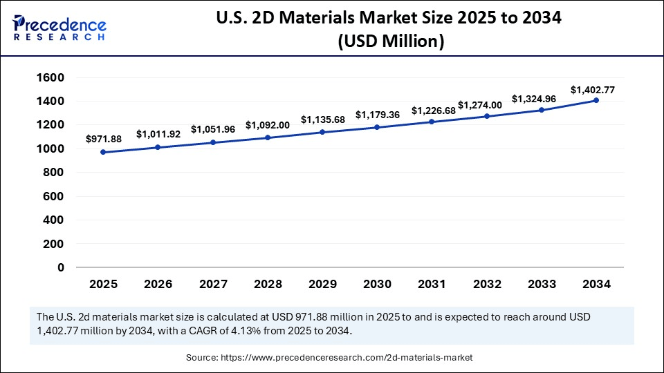
The U.S. 2D materials market size is exhibited at USD 971.88 million in 2025 and is projected to be worth around USD 1,402.77 million by 2034, growing at a CAGR of 4.13% from 2025 to 2034.

Which region dominated the global 2D Materials Market with a 52% share in 2024?
North America led the global market with the highest share of 52% in 2024. The leadership in the region is initiated by a strong R&D ecosystem, a strong semiconductor business, and extensive industrial use of sophisticated materials in electronics, energy, healthcare, and the automobile industries. North America has a robust innovation hub of 2D materials because of the presence of robust academic-industrial partnerships and top graphene and TMD commercialization efforts. Government incentives and favorable policies to encourage the use of clean energy and green technologies improve the speed of adoption, especially in the fields of energy storage, fuel cells, and next-generation batteries.
The U.S. enjoys the benefits of having consolidated large-scale technology companies, research centers, and government-funded initiatives to assist in the development and application of 2D materials. Moreover, an increase in the volume of automobile production, along with a trend towards electric vehicles and renewable energy infrastructure in the country, is increasing the utilization of 2D materials in batteries and supercapacitors, and also in catalytic systems. The regulatory landscape in the U.S. is also favorable, and the efforts are towards making the country green, sustainable, and pollution-free.

Why is Europe undergoing the Fastest Growth in the 2D Materials Market?
Europe is estimated to grow at the fastest CAGR during the forecast period, due to the presence of the most advanced R&D infrastructure, a positive government incentive, and sector-wide sustainability and advanced technologies investments. European pressure to realize a sustainable and low-carbon economy also contributes to the use of 2D materials in energy storage, renewable energy systems, and green electronics. Moreover, increasing investments of state and commercial organizations are opening prospects of mass production and commercialization of such materials.
Countries such as Germany, the United Kingdom, and France are leading the way by investing heavily in nanotechnology and materials science projects, often in conjunction with academia and industry consortia. The EU programs, such as Horizon Europe, are funded to facilitate innovation and commercialization as well as cross-border cooperation on a long-term basis. Research excellence through this ecosystem also helps lessen the use of imported technology by developing local capacity. Europe is becoming the fastest-growing market of 2D materials due to a combination of sustainable policies, innovative research, and industrialization, which are also contributing to a worldwide trend of more high-tech and environmentally friendly technologies.
How is the Opportunistic Rise of Latin America in the 2D Materials Market?
Latin America is experiencing a strategic rise in the market, with growth mainly driven by increasing government investment in materials sciences and nanotechnology. The region is seeing early adoption in research for potential uses in sensors and energy storage, especially in Brazil and Mexico. The market is currently small, facing challenges like high production costs and a less developed industrial application base compared to other global regions.
Brazil serves as a key hub for 2D materials research in Latin America, supported by a vibrant scientific community and advanced research facilities. The market for materials like graphene is mainly driven by academic and government-funded research efforts. The focus is on early-stage applications and potential integration into local industrial sectors, although commercial use remains limited. The market is expected to expand as research results lead to viable commercial applications.
What Potentiates the Growth of the Middle East and Africa 2D Materials Market?
The market in the Middle East and Africa (MEA) is driven by government efforts to diversify economies through investments in R&D and technology. Countries like the UAE and Saudi Arabia are creating research centers focused on nanotechnology and advanced materials. The main applications being explored are water purification/desalination and energy storage solutions, using the unique properties of 2D materials like graphene and transition metal dichalcogenides (TMDs) to tackle regional challenges.
Saudi Arabia is leading the MEA region in 2D materials research and development, driven by substantial investment in R&D. Institutions such as King Abdullah University of Science and Technology (KAUST) are at the forefront of research on graphene and related materials for applications in solar energy, water filtration, and advanced electronics. The focus is on leveraging these materials to innovate solutions for local environmental and industrial needs.
Why is Asia Pacific Considered a Notably Growing Area?
Asia Pacific is considered a notably growing area in the 2D materials market due to its strong focus on technological innovation and rapid industrialization, with countries like China, Japan, and South Korea leading the way in advanced electronics, energy storage, and semiconductor manufacturing. The region is home to some of the world's largest technology companies, which are investing heavily in the development and application of 2D materials, such as graphene, for next-generation devices, flexible displays, and renewable energy solutions. Furthermore, government initiatives and increasing R&D funding across Asia Pacific are driving advancements in material production techniques, making it a key hub for the commercialization of 2D materials.
Value Chain Analysis
Research and Development
This stage focuses on discovering new 2D materials beyond graphene, understanding their properties, and developing synthesis methods.
- Key Players: Graphenea and Versarien.
Manufacturing and Production
This stage focuses on translating lab production into scalable, cost-effective manufacturing with quality control.
- Key Players: Graphenea, NanoXplore, and Thomas Swan.
Distribution and Supply Chain Management
This stage ensures reliable delivery of materials to users, often through specialized logistics and direct sales.
- Key Players: ACS Material and American Elements.
Application and Service Integration
Integrating 2D materials into higher-level components and devices across various sectors.
- Key Players: Haydale. Versarien plc, NanoXplore Inc.
Post-Sale Support and Commercialization
Providing technical support and consultation to accelerate integration and commercial use.
- Key Players: Graphenea, NanoXplore.
Top Companies in the 2D Materials Market and Their Offerings

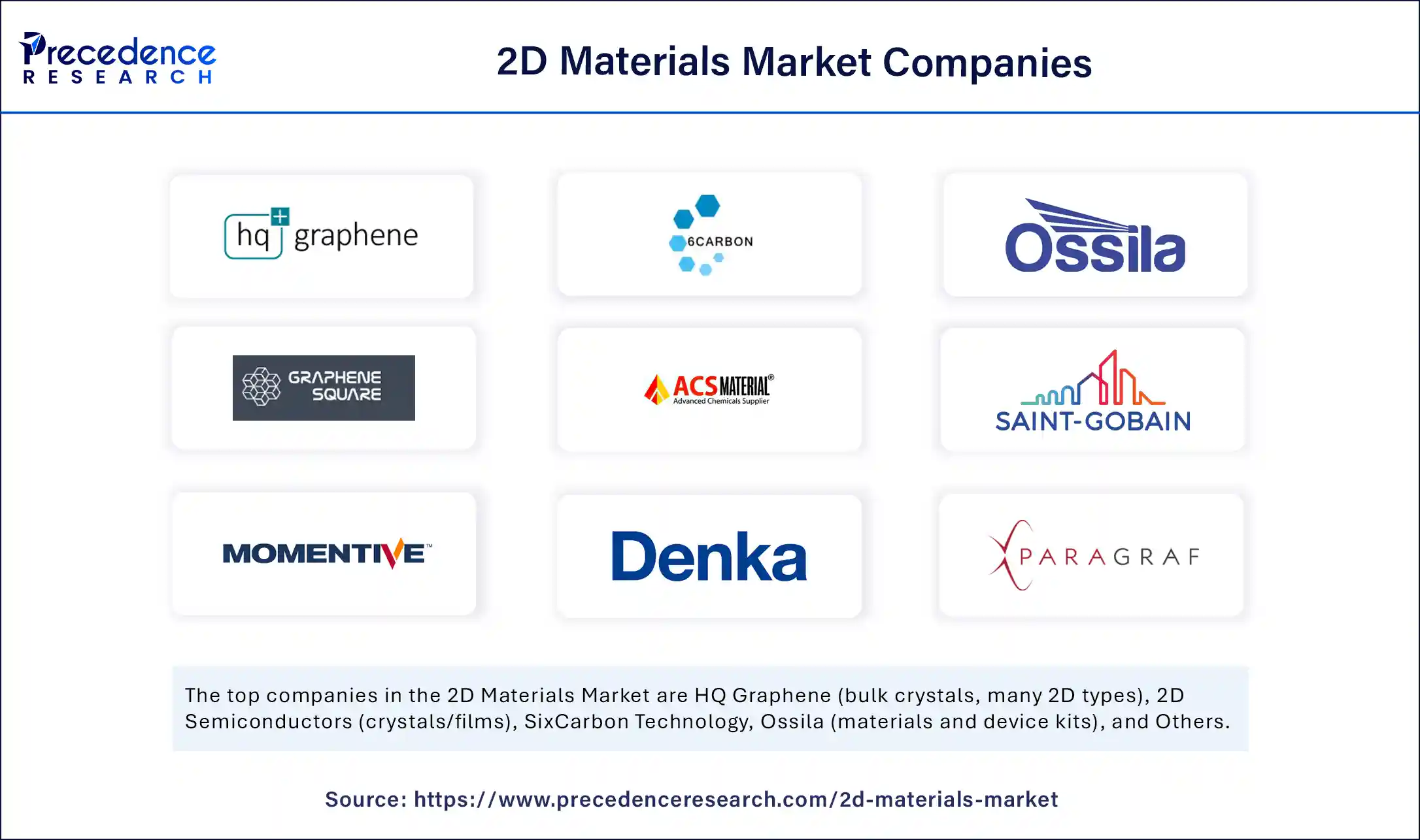
- HQ Graphene : Bulk single crystals of graphene, h-BN, and various TMDs for R&D.
- 2D Semiconductors:Crystals and films of graphene, TMDs, and h-BN for R&D labs.
- Ossila: 2D materials, device kits, and characterization equipment for rapid prototyping.
- Saint-Gobain :Large-scale production of various Boron Nitride (BN) materials.
- Oxford Instruments:Equipment for depositing and fabricating 2D materials (CVD, ALD, etc.).
Other Key Players
- SixCarbon Technology
- Graphene Square
- ACS Material
- Momentive
- Denka
- Paragraf
- Aixtron
- Applied Materials
- ULVAC
- Angstron Materials/Global Graphene Group
- Blackleaf/Advanced Graphene Products
- Tiankang/Jicang
- LayerOne/Paragraf partners
- 2D Fab AB
- BNNano
Recent Developments
- In June 2025, Pennsylvania State University scientists constructed the first CMOS-based computer made completely of two-dimensional materials, and not silicon. This breakthrough demonstrated the promise of nanoscale materials to overcome traditional semiconductors, a key advance toward smaller, faster, and more energy-efficient electronic devices in the technological applications of the future. (Source: https://m.economictimes.com )
- In November 2024, the 2D-Pilot Line is a European Commission-funded semiconductor integration of 2D materials. It was based on the previous 2D-EPL program, which provided end-to-end photonics prototyping and electronics, promoted the use of graphene and TMDCs in industry by improving process maturity and scaling novel technologies throughout the European semiconductor community. (Source: https://graphene-flagship.eu )
- In October 2024, Imperial College London initiated a spinout, 2D Nano, which aimed to commercialise the production of 2D materials. The company employed USD 2.36 million in private capital to expand its production of graphene, boron nitride, and molybdenum disulfide, and now it can produce products reinforced with graphene on a large scale of 100,000 tonnes per year.(Source: https://www.imperial.ac.uk )
Segment Covered in the Report
By Material Family
- TMDs (MoS?, WS?, WSe?, MoSe?)
- MXenes (Ti?C?T?, etc.)
- Hexagonal Boron Nitride (h-BN)
- Black Phosphorus/Phosphorene
- Other 2D Oxides/Nitrides/Carbides
By Application
- Electronics and Optoelectronics
- Energy Storage and Conversion (batteries, supercaps, catalysts)
- Thermal/EMI and Barrier Films
- Sensors (bio/chemical, NEMS)
- Filtration/Membranes and Coatings
By Synthesis/Format
- CVD/MOCVD/ALD Wafers and Films
- Bulk/Single-Crystal Sources (research-grade crystals)
- Solution-Processed Inks/Dispersions
- Mechanical/Liquid Exfoliation
By End User
- Semiconductor and Optoelectronic Manufacturers
- Research Institutes and Foundries
- Energy and Storage OEMs
- Advanced Coatings/Films Converters
- Life Sciences and Sensors
By Region
- Asia Pacific
- Europe
- North America
- Middle East and Africa
- South America
For inquiries regarding discounts, bulk purchases, or customization requests, please contact us at sales@precedenceresearch.com
Frequently Asked Questions
Tags
Ask For Sample
No cookie-cutter, only authentic analysis – take the 1st step to become a Precedence Research client
 Get a Sample
 Table Of Content


 sales@precedenceresearch.com
 +1 804-441-9344
 Schedule a Meeting